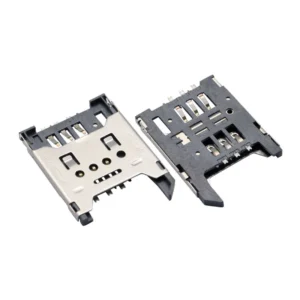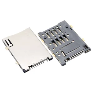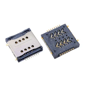
Nano SIM vs Micro SIM Socket Design: Height, Contact Force and PCB Keep-Out

Nine hundredths of a millimetre, and why it matters
Nano SIM (4FF) is 0.67 mm thick. Micro SIM (3FF) is 0.76 mm. The difference is 0.09 mm — thinner than a sheet of paper, and smaller than most people would consider a design variable.
It is the single number that decides whether a socket works reliably in the field, because contact force in a card socket comes from beam deflection. Nine hundredths of a millimetre less deflection means less normal force on every contact, and less force means less ability to break through the oxide and contamination film on the card pads.
This article covers what changes between the two designs, how socket makers compensate, and the adapter practice that quietly destroys sockets.
The two envelopes
| Parameter | 4FF (Nano SIM) | 3FF (Micro SIM) | Consequence |
|---|---|---|---|
| Card length | 12.3 mm | 15.0 mm | Socket body shorter; different board area |
| Card width | 8.8 mm | 12.0 mm | Narrower contact row spacing |
| Card thickness | 0.67 mm | 0.76 mm | Contact force budget |
| Contact layout | ISO 7816, same six positions | ISO 7816, same six positions | Electrically identical |
| Typical socket height | 1.25–1.5 mm | 1.4–2.0 mm | Nano saves vertical space |
| Typical footprint | ~14 × 13 mm incl. stroke | ~17 × 16 mm incl. stroke | Nano saves board area |
The electrical interface is identical, which is what makes the substitution error so common. A designer who has qualified a micro SIM socket and switches to nano for board space assumes the only change is mechanical envelope. The electrical part is indeed unchanged. The mechanical part is the problem.
Beam deflection and the force budget
A card socket contact is a cantilever spring. The contact force depends on how far the beam is deflected from its free position, and on the beam’s stiffness:
Contact force ≈ stiffness × deflection
A typical SIM contact has a stiffness in the range of 200–400 N/m. With a 0.67 mm card and a designed free height that produces roughly 0.3 mm of deflection, the normal force lands in the 0.06–0.12 N range per contact before pre-load. Socket designers add pre-load to lift this into the working range of roughly 0.2–0.5 N per contact.
| Card thickness | Beam deflection | Relative contact force | Effect on oxide breakthrough |
|---|---|---|---|
| 0.76 mm (3FF) | Full design value | 100% | Designed margin |
| 0.67 mm (4FF) | About 12% less | About 88% | Still adequate if the socket was designed for 4FF |
| 0.67 mm card in a 3FF socket | About 12% less | About 88% | Reduced margin; contamination risk rises |
| 0.76 mm card in a 4FF socket | About 13% more | About 113% | Beam over-deflected; risk of permanent set |
The asymmetry matters. An under-thick card produces a mild loss of margin that may never show up. An over-thick card produces over-deflection, and beams that are pushed past their elastic limit do not spring back. The socket is then permanently weak on those contacts, and the failure appears later as intermittent contact with a card that is exactly the right thickness.
The adapter trap
This is where the 0.09 mm becomes expensive.
A nano-to-micro adapter exists so that a 4FF card can be used in a 3FF socket. The adapter adds a carrier frame around the small card. That frame has its own thickness, and its own tolerance — commonly ±0.05 mm, sometimes worse on low-cost parts.
The arithmetic is unforgiving:
| Stack | Nominal thickness | Worst case | Result in a 4FF socket |
|---|---|---|---|
| 4FF card alone | 0.67 mm | 0.69 mm | Correct |
| 4FF card + adapter | 0.67 + adapter | Often 0.80–0.90 mm | Over-deflects the beam by 20–35% |
| 3FF card alone in a 3FF socket | 0.76 mm | 0.78 mm | Correct |
A 0.85 mm stack in a socket designed for 0.67 mm puts every contact beam past its intended deflection. The insertion force rises noticeably — users report that the card “needs a hard push” — and some beams take a permanent set.
The failure does not appear immediately. It appears months later, when the same socket is used with a correct 0.67 mm card and one or two contacts no longer have enough force. That is a warranty return with no obvious cause, and the adapter has long since been removed.
If you must support both form factors, do it with a socket whose compliance range is explicitly specified to cover 0.67–0.80 mm, and validate contact resistance with the adapter installed at the worst-case thickness. Do not assume that because the card fits, the stack is acceptable.
PCB keep-out: the part that changes layout
| Feature | 4FF socket | 3FF socket |
|---|---|---|
| Card insertion stroke | ~13 mm from socket edge | ~16 mm from socket edge |
| Card overhang when seated | Shorter; card sits almost fully inside the body | Longer; more card protrudes |
| Keep-out for components | Socket footprint + stroke + 0.5 mm | Socket footprint + stroke + 0.5 mm |
| Typical layout error | Placing a tall component in the stroke path | Same, but the longer stroke eats more board |
The keep-out error is not in the footprint; it is in the stroke. A push-push socket needs the card to travel its own length to eject. Designers copy the footprint from the datasheet, place a capacitor 2 mm from the socket edge, and discover at mechanical integration that the card cannot come out.
The nano socket makes this easier — the stroke is shorter — but it does not eliminate it. Add the stroke to the footprint before placing anything.
Height: where the 4FF advantage is real
The genuine benefit of switching to nano is vertical. A 4FF socket at 1.25 mm versus a 3FF socket at 1.4–2.0 mm is a saving of 0.15–0.75 mm, which in a thin handheld is the difference between fitting and not fitting.
That saving comes with the contact-force trade-off described above. The lower the socket profile, the less room there is for the terminal beam to develop deflection. A 1.25 mm socket cannot have the beam travel of a 2.0 mm socket, so its contact force depends more heavily on pre-load and on the card being at nominal thickness.
| Socket height | Available beam travel | Tolerance to card thickness |
|---|---|---|
| 1.25 mm | Lowest | Narrow — nominal card only |
| 1.4 mm | Moderate | Moderate |
| 1.5 mm | Good | Good — practical for field-serviceable products |
If the card will be inserted by a user, in a product that sees temperature extremes or contamination, the 1.5 mm option is worth the 0.25 mm it costs. The 1.25 mm part is for devices where the card is fitted at the factory.
Design checklist
| Decision | State explicitly |
|---|---|
| Card form factor | 4FF or 3FF, not “SIM” |
| Thickness compliance range | Required range in millimetres, including adapter tolerance if used |
| Contact force | Minimum per contact, at the thin end of the card tolerance |
| Insertion force | Maximum, at the thick end of the card tolerance |
| Socket height | Selected against beam travel, not just available space |
| Stroke keep-out | Footprint plus card length, marked on the layout |
| Adapter use | Either forbidden, or validated at worst-case thickness |
FAQ
Can a nano SIM socket take a micro SIM card with an adapter? Mechanically it can be forced, but the adapter stack typically reaches 0.80–0.90 mm against a 0.67 mm design, which over-deflects the contact beams and can permanently weaken them.
Is the electrical interface different between 4FF and 3FF? No. Both use the ISO/IEC 7816 six-contact arrangement in the same positions. Only the mechanical envelope changes.
Why does my socket feel stiff with an adapter installed? Over-deflection. The beam is being pushed further than it was designed to travel, which raises insertion force and risks permanent set.
Does a thinner card mean lower contact force? Yes, by roughly the ratio of the deflection change — about 12% for the 0.67 versus 0.76 mm case. A socket designed for 4FF builds in enough pre-load to absorb that.
Which height should I choose for a field-serviceable product? 1.5 mm where space allows. The extra 0.25 mm buys beam travel, which buys tolerance to card thickness and contamination.
What is the most common layout mistake? Forgetting the insertion stroke. The socket footprint fits, but the card cannot travel far enough to eject because a component was placed in its path.
SIM Card Connectors for this design
View all 41 parts →