
USB Connector for PCB: Design Guidelines
USB Connector for PCB: Design Guidelines
Introduction
USB connectors look simple on a schematic — 4 to 24 pins, some power, some data, connect them and move on. On a PCB, they are among the most demanding components to route correctly. The same footprint that carries 480 Mbps USB 2.0 might need to handle 10 Gbps SuperSpeed differential pairs, 5A of VBUS current, and ESD strikes from repeated cable insertions — all within a 8.3mm × 2.4mm connector body.
This article covers the PCB design guidelines that matter: connector selection (SMT vs. through-hole, top-mount vs. mid-mount), high-speed signal routing, power delivery layout, ESD protection, and the common mistakes that show up in design reviews and compliance testing failures.
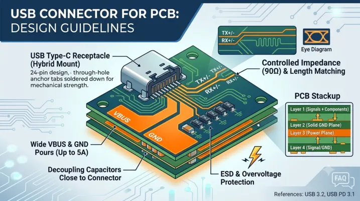
1. USB Connector Types for PCB Mounting
1.1 USB Type-C Receptacle Variants
| Mounting Style | Description | Best For | Limitations |
|---|---|---|---|
| Top-mount (SMT) | Sits on PCB surface, all SMT pads | Standard designs, 1.6mm PCBs | Mechanical stress on pads during insertion |
| Mid-mount (SMT) | Centered in PCB thickness (cutout required) | Thin devices (< 5mm), tablets, phones | Complex PCB cutout, higher assembly cost |
| Vertical | Stands perpendicular to PCB | Test equipment, front-panel access | Taller profile, harder to waterproof |
| Hybrid (SMT + TH) | Signal pins SMT, anchor tabs through-hole | High-durability applications | Larger footprint, through-hole adds cost |
| Dual-row SMT | Two rows of SMT pads | Space-constrained, premium designs | Harder to inspect solder joints |
1.2 USB-A and Micro-B
While USB-C is the modern standard, USB-A receptacles still appear in industrial equipment, test instruments, and legacy designs. Key PCB considerations:
- USB-A vertical: Common for front panels. Through-hole mounting provides mechanical strength.
- USB-A right-angle (SMT): Standard for PC motherboards and hubs. Requires cutout or edge placement.
- Micro-B 3.0: Wide connector body with two rows of contacts. SMT-only; susceptible to pad lifting if cable is pulled laterally.
2. Connector Footprint Design
2.1 Pad Geometry
The USB-C connector footprint is specified by USB-IF. However, manufacturers offer variants with different pad arrangements. Key dimensions:
| Parameter | Typical Value | Notes |
|---|---|---|
| Connector body width | 8.34 mm | Nominal, varies ±0.05 mm by manufacturer |
| Connector body depth (PCB edge to back) | 7.4-9.0 mm | Depends on mounting style |
| Pin pitch (signal row) | 0.50 mm | Standard pitch for 24-pin USB-C |
| Pad width (signal) | 0.30 mm | Narrow — requires precise solder paste stencil |
| Pad length | 1.0-1.5 mm | Longer pads improve mechanical strength |
2.2 Anchor Tabs and Mechanical Retention
Pure SMT USB-C connectors rely on solder pad adhesion for mechanical retention. USB-IF specifies 10,000 insertion cycles — but that assumes proper PCB design:
- Through-hole anchor tabs: The single most effective reliability improvement. Two through-hole posts at the connector shell corners transfer insertion/withdrawal forces to the PCB structurally, not through solder joints.
- Additional SMT anchor pads: Some connectors include large SMT pads on the shell for extra solder area.
- PCB cutout: A slot in the PCB allows the connector to sit flush with the board edge, reducing the lever arm on solder joints.
For designs expecting more than 1,000 insertions, use a connector with through-hole anchors. For consumer devices with lower expected cycles, pure SMT is acceptable if the pad design follows manufacturer recommendations exactly.
2.3 Keep-Out Zones
The area immediately behind the connector is critical:
- No components within 1.5 mm of the connector body on the top layer — the mating plug requires clearance
- No tall components (> 2 mm) within 5 mm — cable strain relief and plug body extend beyond the connector face
- Keep-out on inner layers under the connector: Avoid routing unrelated signals under the connector footprint. The connector body can capacitively couple noise onto nearby traces.
3. High-Speed Signal Routing
3.1 Differential Pair Routing Rules
USB SuperSpeed signals (TX1+/-, TX2+/-, RX1+/-, RX2+/-) operate at up to 10 Gbps per lane (USB 3.2 Gen 2) or 20 Gbps (USB4 Gen 3). At these speeds, every millimeter of trace matters.
| Parameter | USB 3.2 Gen 1 (5 Gbps) | USB 3.2 Gen 2 (10 Gbps) | USB4 Gen 3 (20 Gbps) |
|---|---|---|---|
| Differential impedance | 90 Ω ±15% | 90 Ω ±10% | 85 Ω ±10% |
| Intra-pair skew | < 15 ps | < 10 ps | < 5 ps |
| Inter-pair skew | < 100 ps | < 50 ps | < 25 ps |
| Max trace length (FR-4) | 150 mm | 100 mm | 50-75 mm |
| Max vias per pair | 4 | 2 | 0-1 |
3.2 Impedance Control
Achieving 85-90 Ω differential impedance on standard FR-4:
- Microstrip (top/bottom layer): Use a ground plane on layer 2. For 0.15mm trace width with 0.15mm spacing on 0.1mm prepreg, Zdiff ≈ 90 Ω.
- Stripline (inner layer): Sandwiched between two ground planes. Requires wider traces for the same impedance. Lower loss than microstrip but adds two vias.
- Critical rule: Do not change reference planes along a differential pair’s path. If a layer change is unavoidable, place ground stitching vias within 2mm of the signal vias.
3.3 Length Matching
Intra-pair length matching compensates for the different path lengths within a differential pair. Even small mismatches create common-mode noise that degrades signal integrity:
- Route differential pairs together from connector to IC
- Add serpentine (trombone) structures near the mismatch source, not at the end of the trace
- Serpentine segment length: 3× trace width minimum to avoid coupling between adjacent segments
- After length matching, verify with post-layout simulation if possible
3.4 Grounding and Return Path
Each SuperSpeed differential pair has adjacent ground pins on the USB-C connector. These ground connections must extend to a solid ground plane:
- Ground vias within 1 mm of each connector ground pin
- Uninterrupted ground plane under all SuperSpeed routing
- No splits or gaps in the reference plane under differential pairs
- If using a 4-layer board: Layer 1 (signals), Layer 2 (solid GND), Layer 3 (power), Layer 4 (signals + GND fill)
3.5 USB 2.0 D+/D- Routing
At 480 Mbps, USB 2.0 is forgiving compared to SuperSpeed, but still needs care:
– 90 Ω differential impedance
– Keep away from noisy digital signals (clock lines, switching regulators)
– Do not route parallel to SuperSpeed pairs at close distance — the 5 Gbps signals can couple onto USB 2.0
– USB 2.0 traces can be longer (up to 300mm) without active re-drivers
4. Power Delivery Layout
4.1 VBUS and GND Routing
USB-C VBUS can carry up to 5A at 48V (240W with PD 3.1 EPR). Even at more common levels (5A at 20V = 100W), trace design matters:
| Current | Minimum Trace Width (1 oz Cu, 10°C rise) | Recommended Width |
|---|---|---|
| 1A | 0.3 mm | 0.5 mm |
| 3A | 1.5 mm | 2.5 mm |
| 5A | 3.5 mm | 5.0 mm or copper pour |
Use copper pours instead of traces for VBUS and GND where possible. On a 4-layer board, dedicate at least one inner layer to a solid ground plane and use wide pours on the power layer.
4.2 Decoupling Capacitors
Place bypass capacitors close to the connector VBUS pins:
– 10 µF ceramic (X5R or X7R) within 5 mm of the connector
– 0.1 µF ceramic in parallel for high-frequency decoupling
– Additional bulk capacitance (22-100 µF) near the power input to the PD controller or voltage regulator
– Capacitor voltage rating: 2× the maximum expected VBUS voltage (50V for 20V systems, 100V for EPR)
4.3 Thermal Management
At 5A, even a well-designed PCB trace dissipates heat:
– 10 mΩ trace at 5A = 0.25W — fine for a single connector
– Multiple USB-C ports on one board: aggregate power dissipation can be several watts
– Place temperature-sensitive components (crystals, sensors) away from VBUS current paths
– For high-power designs, consider 2 oz copper on power layers
4.4 Creepage and Clearance for EPR (48V)
USB PD 3.1 EPR at 48V requires attention to PCB safety spacing:
| Voltage | Creepage (uncoated, pollution degree 2) | Clearance |
|---|---|---|
| 20V (SPR) | 0.5 mm | 0.5 mm |
| 48V (EPR) | 1.2 mm | 1.0 mm |
The 0.5 mm pin pitch of USB-C connectors is sufficient for 20V but marginal for 48V creepage between adjacent VBUS and signal pins. For EPR designs, consider conformal coating to improve the effective creepage distance.
5. ESD and Overvoltage Protection
5.1 ESD Protection Requirements
USB connectors face frequent ESD strikes during cable insertion. The human body model (HBM) discharge can reach 8-15 kV. Protection is mandatory:
| Signal Type | Protection Device | Key Parameters |
|---|---|---|
| SuperSpeed (TX/RX) | Low-cap TVS diode | < 0.5 pF capacitance, > 8 kV contact |
| USB 2.0 (D+/D-) | TVS diode array | < 3 pF, > 8 kV contact |
| CC / SBU | TVS diode | < 10 pF, > 8 kV contact |
| VBUS | TVS + OVP | > 15 kV contact, > 30V clamp for SPR |
5.2 TVS Diode Placement
- Place TVS diodes as close to the connector as possible — within 10 mm
- Route the protected trace through the TVS diode pad (no stubs)
- Connect TVS ground directly to the connector ground pins, then to the ground plane
- Do not share TVS ground vias with high-current VBUS return paths
5.3 Overvoltage Protection on VBUS
A faulty USB-C charger can output 20V onto a circuit designed for 5V. Protection options:
– Dedicated OVP IC: Monitors VBUS and disconnects if voltage exceeds threshold
– TVS + fuse: TVS clamps overvoltage, fuse blows if sustained — simple but one-shot
– Ideal diode controller: Provides reverse current protection and OVP in one IC
5.4 CC and SBU Protection
The CC pin is particularly vulnerable — it connects directly to the PD controller and is exposed on the connector. A short from VBUS to CC (possible with a damaged cable or liquid ingress) can destroy the PD controller. Use a TVS diode rated for the full VBUS voltage range, not just the CC voltage (typically 5V).
6. Common Design Mistakes
6.1 Missing or Incorrect CC Pull-Down Resistors
Every USB-C sink port needs a 5.1 kΩ pull-down resistor to ground on each CC pin. Missing this resistor means the source will not detect the sink and will not supply power. Using the wrong value (e.g., 56 kΩ instead of 5.1 kΩ) can cause the source to supply only default USB current (500 mA / 900 mA) instead of 3A.
6.2 Floating Shield Connection
The USB-C connector shield (metal shell) should connect to PCB ground — but how matters:
– Direct connection: Best for EMI, but creates ground loop risk
– RC connection (100 nF + 1 MΩ parallel to ground): Reduces ground loop while providing RF path
– Decision rule: Battery-powered devices can directly connect the shield. Mains-powered devices with multiple ground paths should use the RC network.
6.3 Insufficient Ground Vias Under the Connector
USB-C connectors have multiple ground pins that must connect to a low-impedance ground plane. A single via per ground pin is minimum; two vias per pin is recommended. Without adequate grounding, return currents find unintended paths, increasing EMI and degrading signal integrity.
6.4 Routing Sensitive Signals Under the Connector
The USB-C connector body is not shielded on the bottom. Routing a sensitive analog trace (audio, sensor, clock) under the connector footprint couples noise from the VBUS and SuperSpeed signals. Keep all layers clear under the connector body.
6.5 Forgetting the Unmated State
A USB-C port that is not connected to anything still has exposed pins. ESD can strike an unmated port just as easily as during insertion. Protection devices must handle the unmated state — which means TVS diodes on all exposed pins, not just those used during operation.
7. Layer Stackup Recommendations
7.1 4-Layer Stackup (Cost-Optimized)
| Layer | Assignment | Notes |
|---|---|---|
| Top | Signals + components | USB SuperSpeed pairs, short routes |
| L2 | Solid GND plane | Uninterrupted under all USB routing |
| L3 | Power plane (VBUS, VCC) | Copper pours for power distribution |
| Bottom | Additional signals | USB 2.0, CC, low-speed signals |
7.2 6-Layer Stackup (Performance)
| Layer | Assignment | Notes |
|---|---|---|
| Top | Critical signals | SuperSpeed pairs, no vias to connector |
| L2 | GND plane | Reference for top-layer microstrip |
| L3 | Inner signal routing | Additional SuperSpeed pairs (stripline) |
| L4 | Power plane | Split for VBUS, VCC, VDD |
| L5 | GND plane | Reference for bottom layer |
| Bottom | Low-speed signals | USB 2.0, I2C, GPIO |
7.3 Key Stackup Rules
- Always have a continuous ground plane adjacent to every signal layer carrying USB SuperSpeed
- Avoid routing SuperSpeed on layers that reference a split or slotted plane
- Use symmetric stackup to prevent board warpage, which can crack SMT connector solder joints
8. Manufacturing and Assembly
8.1 Solder Paste Stencil Design
The 0.50 mm pin pitch of USB-C connectors requires a precise stencil:
– Stencil thickness: 0.10-0.12 mm (4-5 mil)
– Aperture reduction: 10-15% for signal pads to prevent bridging
– Home-plate or rounded aperture shapes improve paste release
– Step stencil may be needed if other components require thicker paste
8.2 Inspection
- X-ray inspection for hidden solder joints under the connector body (mid-mount and dual-row styles)
- Visual inspection of side fillets for top-mount connectors
- Electrical test: continuity check on all pins, especially VBUS and GND which have multiple parallel pins
8.3 Rework Considerations
USB-C connectors are difficult to rework:
– The fine pitch and multiple rows make hot-air rework challenging without damaging adjacent components
– Pre-heat the board to 100-120°C before applying hot air to the connector
– Expect to replace the connector, not reflow it — the internal plastic body can deform during rework
– Design with test points on all critical signals so functionality can be verified before the connector is attached
9. Pre-Compliance Testing on Your PCB
Before sending a design to a USB-IF compliance lab, perform these tests in-house:
9.1 Signal Integrity
- TDR measurement on SuperSpeed pairs to verify differential impedance
- Eye diagram measurement at the connector (requires SMA-to-USB-C test fixture)
- Near-end crosstalk (NEXT) between adjacent SuperSpeed pairs
9.2 Power Delivery
- VBUS voltage drop at full rated current (measure at connector, not at regulator output)
- Inrush current measurement during hot-plug (should be < 5A peak for SPR)
- PD protocol trace (capture CC line with logic analyzer to verify PD negotiation)
9.3 ESD
- Contact discharge at 8 kV to connector shell and exposed pins (unmated)
- Verify device continues normal operation after ESD strike (no latch-up, no reset)
- Air discharge at 15 kV for connectors accessible to users
FAQ
Q: Do I need to route all four SuperSpeed pairs if my design only uses USB 3.2 Gen 1 (5 Gbps)?
A: No. USB 3.2 Gen 1 uses only one TX pair and one RX pair. The other two SuperSpeed pairs can be left unconnected. However, if the connector will be used for Alternate Mode or USB4 in the future, route all four pairs now.
Q: What is the minimum PCB thickness for a USB-C mid-mount connector?
A: Mid-mount connectors are designed for specific PCB thicknesses, typically 0.8mm, 1.0mm, or 1.2mm. The connector datasheet specifies the exact thickness. Using the wrong PCB thickness means the connector will not align with the enclosure opening.
Q: Can I route USB SuperSpeed pairs through a connector or flex cable?
A: Yes, but each additional connector or flex transition adds insertion loss and impedance discontinuities. Budget roughly 1-2 dB of loss per connector at 5 GHz. For USB4 at 20 Gbps, minimize the number of transitions and use impedance-controlled flex circuits.
Q: How do I handle the shield connection on an isolated USB port (e.g., medical device)?
A: For galvanically isolated USB (medical, some industrial), the shield must not create a ground path that bypasses the isolation barrier. Options: (1) Float the shield entirely (EMI risk), (2) Connect shield to the isolated ground through an RC network, (3) Use an isolated USB transceiver with separate shield management. Consult IEC 60601 for medical isolation requirements.
References: USB Type-C Cable and Connector Specification R2.4, USB 3.2 Specification, USB4 Specification, IPC-2221 (Generic Standard on Printed Board Design), IEC 61000-4-2 (ESD Immunity).