
Stacked USB Connector Footprint & Pinout: PCB Design Reference
Stacked USB Connector Footprint & Pinout: PCB Design Reference
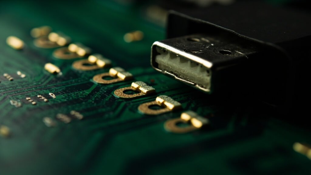
If you’re laying out a PCB with a stacked USB connector, the footprint is the first thing you need to get right — and the last thing you want to debug after the boards come back. A misaligned footprint means the connector sits crooked on the board, the panel cutout doesn’t line up, or SMT pads don’t wet properly during reflow.
This reference covers the standard pinouts for stacked USB 2.0 and USB 3.0 Type-A connectors, plus footprint design guidelines that go beyond the datasheet drawing.
Stacked USB 2.0 Type-A Pinout (Dual Port)
A stacked USB 2.0 connector has 8 contacts total — 4 per port:
Upper Port (Top)
| Pin | Signal | Description |
|---|---|---|
| 1 | VBUS | +5V power |
| 2 | D− | USB data, negative |
| 3 | D+ | USB data, positive |
| 4 | GND | Ground |
Lower Port (Bottom)
| Pin | Signal | Description |
|---|---|---|
| 5 | VBUS | +5V power |
| 6 | D− | USB data, negative |
| 7 | D+ | USB data, positive |
| 8 | GND | Ground |
The pin numbering convention varies between manufacturers. Some label pins 1–4 (upper) and 5–8 (lower) as shown above. Others label upper port 1–4 and lower port A1–A4. Always verify against the specific manufacturer’s datasheet — don’t assume numbering.
Important: The upper and lower ports are electrically independent. They share only the connector housing and shell ground. You can route them to separate USB controllers, separate power switches, or even use one port for USB host and the other for USB device (OTG) — the connector doesn’t care.
Stacked USB 3.0 / 3.1 Gen1 Type-A Pinout (Dual Port)
A stacked USB 3.0 connector has 18 contacts total — 9 per port:
Upper Port (Top)
| Pin | Signal | Description |
|---|---|---|
| 1 | VBUS | +5V power |
| 2 | D− | USB 2.0 data, negative |
| 3 | D+ | USB 2.0 data, positive |
| 4 | GND | Ground |
| 5 | SSRX− | SuperSpeed receive, negative |
| 6 | SSRX+ | SuperSpeed receive, positive |
| 7 | GND_DRAIN | Ground for SuperSpeed return |
| 8 | SSTX− | SuperSpeed transmit, negative |
| 9 | SSTX+ | SuperSpeed transmit, positive |
Lower Port (Bottom)
| Pin | Signal | Description |
|---|---|---|
| 10 | VBUS | +5V power |
| 11 | D− | USB 2.0 data, negative |
| 12 | D+ | USB 2.0 data, positive |
| 13 | GND | Ground |
| 14 | SSRX− | SuperSpeed receive, negative |
| 15 | SSRX+ | SuperSpeed receive, positive |
| 16 | GND_DRAIN | Ground for SuperSpeed return |
| 17 | SSTX− | SuperSpeed transmit, negative |
| 18 | SSTX+ | SuperSpeed transmit, positive |
Critical note for routing: The SuperSpeed pairs (SSRX and SSTX) are differential pairs. Each pair must be routed as a 90Ω differential transmission line with intra-pair length matching to within 5 mils (0.127mm). The GND_DRAIN pin provides the return current reference for the SuperSpeed signals and should connect to a solid ground plane through a via placed as close as possible to the pin.
Footprint Design Guidelines
DIP (Through-Hole) Footprint
A DIP footprint for a stacked USB connector includes:
1. Signal pin holes (8 or 18): Drill diameter typically 0.8–1.0mm. Finished hole size with plating 0.7–0.9mm. Pad diameter 1.4–1.8mm around each hole.
2. Shell grounding tab holes (2 or 4): Shell grounding tabs are larger than signal pins. Drill diameter 1.2–1.6mm, pad diameter 2.2–2.8mm. These tabs provide both mechanical anchoring and ground connection. Connect them to chassis ground (not signal ground) through a wide copper pour — not a skinny 0.3mm trace.
3. Locating pin holes (optional, 2): Some stacked connectors include plastic locating pins for mechanical registration. Drill diameter 1.5–2.0mm, no pad (these are non-conductive pins). They help align the connector before soldering.
Keepout zone: The area under the connector body should be free of vias and components. The connector sits flush against the PCB, and any components or vias under the body will prevent proper seating or create shorts.
Panel edge clearance: The front face of the connector extends past the PCB edge by 2–4mm. Make sure your panel cutout aligns with this extension and that there’s adequate clearance for the USB plug body outside the panel.
SMT (Surface Mount) Footprint
SMT footprint requirements:
1. Contact pads: Length 1.5–2.5mm, width 0.5–0.8mm (varies by connector manufacturer). The pad dimensions on your PCB should match the manufacturer’s recommended land pattern exactly — don’t improvise. SMT pad geometry affects solder fillet formation and mechanical strength.
2. Paste mask opening: Typically 1:1 with the pad dimensions, or slightly reduced (90–95%) to prevent solder bridging on fine-pitch contacts.
3. Board lock slots (2): If the connector has metal board lock tabs, your PCB needs corresponding slots — not round holes. Slot dimensions per manufacturer’s drawing, typically 1.0mm × 3.0mm or similar. The slot orientation matches the board lock tab geometry.
4. Thermal relief: Don’t use thermal relief (spokes) on the grounding pad connections. The connector shell ground needs the lowest possible thermal path to the ground plane for effective EMI shielding. Full contact to the ground plane is preferred over thermal relief spokes for the shell ground pads.
5. Co-planarity zone: The area where the contact tails sit on the PCB pads must be flat — no solder mask bumps, no via-in-pad (unless filled and capped), no surface contamination. A 0.05mm bump under one contact tail on a stacked connector means that particular contact doesn’t get proper solder fillet formation.
Common Footprint Mistakes
Mistake 1: Mirroring the Pinout
We’ve seen PCB layouts where the lower port pinout was mirrored relative to the upper port — the designer assumed the bottom port was a mirror image. It’s not. Both ports have the same pin order (left to right), just on different rows. Double-check the datasheet pin assignment view — look for the words “top view” or “bottom view” and make sure you’re reading the correct perspective.
Mistake 2: No Ground Pours Under the Connector
The area between the connector and the board edge is typically a mechanical keepout zone with no copper. But the area directly under the connector body (on the PCB surface) should have a ground pour connected to the connector shell ground tabs. This ground pour provides:
- Low-impedance ground return for the signal pins
- EMI shielding (the ground plane under the connector reflects electromagnetic fields back toward the connector shell)
- Mechanical support for the PCB in the connector mounting area
Mistake 3: Single Ground Trace for the Shell
A stacked USB connector shell has 2–4 grounding tabs. Connecting all of them to a single 0.3mm trace to the ground plane creates a high-impedance ground path that makes the shell effectively a floating metal object at RF frequencies. Instead, connect each shell grounding tab to a solid ground plane through a short, wide copper connection — or better yet, place the connector footprint so the shell tabs land directly over a ground plane with no neck-down.
Mistake 4: Via-in-Pad for SMT Contacts Without Filling
An SMT contact pad with an unfilled via in it creates a capillary path that wicks solder away from the pad during reflow. The result is a starved solder joint with poor mechanical strength. If you absolutely must put vias in the contact pads (for space reasons), use filled and capped vias — and verify the coplanarity of the capped surface.
Panel Cutout Guidelines
Single Stacked Connector Cutout
A typical stacked USB 2.0 connector requires a panel cutout of approximately:
- Width: 14.5–15.5mm
- Height: 21.0–22.5mm
These dimensions include clearance for the USB plug body, not just the connector shell. The exact dimensions vary by manufacturer — use the recommended cutout drawing from your connector supplier, not a generic dimension.
Panel Cutout Tolerance
The panel cutout tolerance affects both assembly fit and EMI shielding. If the cutout is too large, the connector shell doesn’t make good contact with the panel for EMI grounding. If it’s too small, the connector won’t fit through the panel during assembly.
Typical recommended tolerances:
- Cutout dimensions: −0/+0.2mm (slightly oversized for easy assembly)
- Cutout position relative to PCB mounting holes: ±0.3mm
For panel-mount connectors with a sealing gasket, the tolerance stackup between the PCB mounting holes, the connector position on the PCB, and the panel cutout must be tight enough to ensure consistent gasket compression around the entire perimeter.
Summary
Stacked USB connector footprints require more attention to detail than single-port footprints because of the additional mechanical constraints: more pins, larger connector body, more ground connections to manage, and tighter alignment requirements with the enclosure panel.
The golden rule: trust the manufacturer’s recommended footprint over generic patterns. A 0.2mm difference in pad geometry between manufacturers can mean the difference between 99% first-pass yield and 85% with rework.
For GSConn stacked USB connector datasheets with detailed footprint drawings, recommended land patterns, and panel cutout dimensions, visit the GSConn technical resources section.