
How to Solder USB Connector — SMT and Through-Hole Methods
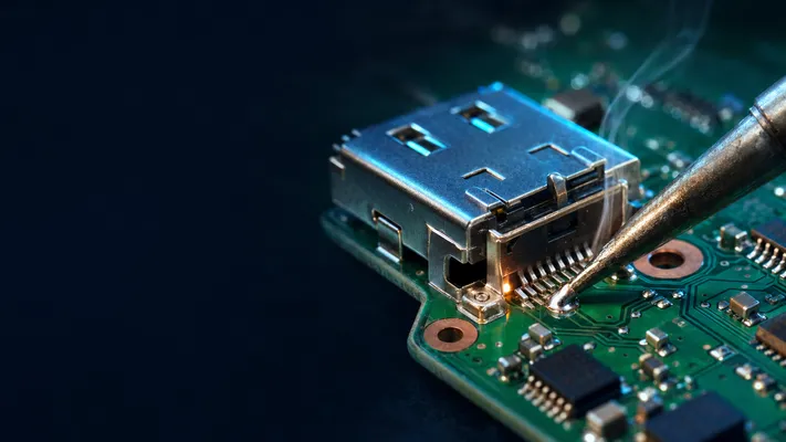
Quick Summary
| Method | Difficulty | Equipment | Best For |
|---|---|---|---|
| Hand-solder through-hole | Easy | Soldering iron (>60W), solder wire, flux | Prototypes, repairs, one-offs |
| Hand-solder SMT (drag method) | Medium | Iron + flux + solder wick | SMT prototypes, small repairs |
| Hot air rework | Medium | Hot air station; 350–380°C typical for lead-free rework | Replacing existing SMT connectors |
| SMT reflow (oven) | Hard | Reflow oven, solder paste, stencil | Production, multiple boards |
1. Through-Hole USB Connector (Easiest)
Tools
- Temperature-controlled soldering iron, 60–80W; typical tip setting 350–380°C for lead-free solder or 320–350°C for SnPb solder
- Chisel tip (2.4mm) for shield tabs, conical tip (0.8mm) for pins
- Lead-free solder (SAC305 Sn96.5/Ag3.0/Cu0.5), 0.5–0.8mm diameter
- No-clean flux pen or paste
- Desoldering pump (solder sucker) for mistakes
Step-by-Step (USB 2.0 Type-A, 4-pin through-hole)
- Pre-tin pads: Apply flux. Lightly tin all PCB pads (thin coat only — too much solder fills the hole and connector won’t seat flush).
- Insert connector: Push connector pins through PCB holes until housing sits flush on PCB surface. Check alignment — housing typically should be parallel to PCB edge.
- Solder one corner tab first: Touch iron to shield tab + pad, feed solder until fillet forms around tab. Let cool 3 seconds. This anchors the connector.
- Solder opposite corner tab: Check connector alignment before soldering. If misaligned, reheat first tab and adjust.
- Solder pin row: 4 pins (VBUS, D-, D+, GND). about 1–2 seconds per pin at an appropriate tip setting. Lead-free solder typically needs slightly more heat than SnPb and may form a less shiny joint even when acceptable.
- Solder remaining tabs: All 4 shield tabs should have shiny fillets on both sides of PCB.
- Inspect: Each pin should have a cone-shaped fillet (concave, not ball-shaped). No bridges between adjacent pins. Shield tabs fully wetted.
Common Through-Hole Mistakes
| Mistake | Result | Fix |
|---|---|---|
| Too much solder in hole | Connector won’t seat flush | Desolder, wick out excess |
| Shield tab not soldered first | Connector shifts during pin soldering | Always anchor tabs first |
| Cold joint (dull, grainy) | Intermittent connection, high resistance | Reheat with fresh flux |
| Pin bridge | Short circuit | Solder wick or desoldering pump |
| Overheating (>3s per pin) | Plastic housing melts or deforms | Limit dwell time, use flux, and let the connector cool between attempts |
2. SMT USB Connector (Drag Soldering Method)
Tools
- Soldering iron with hoof/bevel tip (about 3mm wide); typical tip setting 330–360°C for lead-free SMT work
- Gel flux (tacky, no-clean)
- Solder wire, 0.5mm diameter
- Solder wick (braid), 2.0mm wide
- Magnifying glass or microscope (0.5mm pin pitch)
Step-by-Step (SMT Type-C, 24-pin, 0.5mm pitch)
- Apply flux: Coat all 24 SMT pads AND connector pins with gel flux. Flux is critical — it prevents bridges and helps solder flow to pads.
- Align connector: Use tweezers. Pins typically should align with pads to within 0.2mm. For 0.5mm pitch Type-C, 0.1mm misalignment causes bridges.
- Tack one corner: Add tiny solder blob to one shield tab pad. Reheat and push connector into place. Let cool. Connector is now anchored but can be nudged by reheating.
- Tack opposite corner: Verify alignment under magnification. If misaligned, reheat first corner and adjust.
- Drag solder pin row: Load hoof tip with small solder ball. Drag tip slowly across pin row (3–5 seconds per side). Surface tension pulls solder from tip to pads, leaving bridges between pins.
- Remove bridges: Apply fresh flux to bridged area. Clean tip thoroughly. Touch solder wick to bridge and heat — excess solder wicks into braid. Repeat until all pins are separated.
- Solder shield tabs: Larger pads need more heat. 4 tabs, 3s each, solid fillets.
- Final inspection: Under magnification — no bridges, all pins wetted (shiny fillet to pad), no tombstoning.
Lead-Free vs SnPb Hand-Soldering Notes
| Solder alloy | Typical tip setting | Notes |
|---|---|---|
| Sn63/Pb37 or Sn60/Pb40 | 320–350°C | Lower melting point; avoid mixing with lead-free process unless repair rules allow it |
| SAC305 lead-free | 350–380°C | Common in RoHS production; needs more flux and slightly longer thermal recovery |
| High-thermal-mass shield tabs | 360–400°C, short dwell | Use a wider chisel tip instead of holding a small tip on the joint too long |
The goal is not to use the highest temperature; it is to transfer heat quickly enough to wet the joint without softening the connector housing or lifting pads.
3. SMT Reflow (Production Method)
Tools
- Reflow oven or hot plate
- Solder paste (SAC305, Type 4 or Type 5, no-clean)
- Stencil (laser-cut stainless steel, 0.1–0.12mm thickness)
- Pick-and-place (manual tweezers for prototypes)
Reflow Profile for SAC305 (Lead-Free)
| Zone | Temperature | Duration | Purpose |
|---|---|---|---|
| Preheat | 25 → 150°C | 60–120s | Evaporate flux solvents, preheat PCB |
| Soak | 150 → 200°C | 60–90s | Activate flux, even temperature across PCB |
| Reflow | 200 → 250°C | 30–60s | Melt solder (peak 235–245°C for SAC305) |
| Cooling | 250 → 100°C | Natural or controlled (<4°C/s) | Solidify joints, avoid thermal shock |
Critical: SAC305 melts at 217°C. Peak temperature typically should exceed 235°C for complete reflow but typically should not exceed 250°C (plastic housing may deform). Time above 217°C: 45–90 seconds.
USB Connector Reflow Notes
- Type-C connectors are heavier than they look (metal shell). Place on bottom side of PCB if dual-sided reflow — connector weight won’t cause tombstoning.
- Plastic housing (PBT Tg 215°C, LCP Tg 280°C) — PBT connectors are safe below 250°C peak but edge-close to Tg. LCP connectors have much more margin.
- Connector typically should be placed flat on PCB — no tilt. Solder paste volume typically should be even across all pads.
4. Hot Air Rework (Replacing Damaged Connector)
Tools
- Hot air station, 350–380°C (typically for lead-free soldering), medium airflow
- Tweezers
- Solder wick
Flux
Preheat PCB: 100°C for 30s from underside (reduces thermal shock).
- Apply flux: Around connector base.
- Hot air: 350°C, nozzle 8–10mm, circular motion around connector (not on connector). Heat until solder glosses.
- Remove: Lift connector with tweezers when solder is fully liquid. Do not pull — connector should lift with zero force. Pulling will tear pads.
- Clean pads: Solder wick to remove old solder. Isopropyl alcohol to clean flux residue.
- Place new connector: Apply fresh solder paste or pre-tin pads. Repeat SMT soldering steps.
5. Temperature Limits by Material
| Material | Max Temperature | Safe for Reflow? | Safe for Hand-Solder? |
|---|---|---|---|
| PBT housing | 220°C (Tg) | ⚠️ (250°C peak is risky) | ✅ (localized heat, <2s per pin) |
| LCP housing | 280°C (Tg) | ✅ (safe at 250°C peak) | ✅ |
| Nylon 66 housing | 255°C (Tg) | ⚠️ (close to limit) | ✅ |
| Gold plating | 1064°C (melt) | ✅ | ✅ |
| FR4 PCB | 130°C (Tg standard) | ✅ (short exposure) | ✅ |
6. GSConn Soldering Recommendations
| Connector Type | Mounting | Recommended Method | Max Hand-Solder Time/Pin |
|---|---|---|---|
| Type-A through-hole | TH | Hand-solder iron, 350°C | 2s |
| Type-C SMT | SMT | Reflow (production), drag-solder (prototype) | 1.5s (0.5mm pitch) |
| Stacked USB | TH | Hand-solder or wave solder | 2s |
| Vertical Type-C | SMT/TH | Reflow (SMT), hand (TH) | 2s (TH pins) |
| Mid-mount Type-C | SMT dual-side | Dual-side reflow only | N/A |
GSConn USB connectors use LCP housing on industrial-grade parts for maximum reflow tolerance (Tg 280°C). Standard PBT connectors are safe for hand-soldering with controlled dwell time. For production soldering, contact GSConn for recommended reflow profiles and stencil aperture designs.
Related reading:
– USB Connector PCB Layout Guide
– DIP vs SMT Stacked USB
– USB Connector Lifespan & Mating Cycles
Technical References for Editorial Review
This article was reviewed for engineering accuracy against commonly used connector and USB ecosystem references, including USB-IF Type-C / USB4 / USB Power Delivery documentation, IEC 60512 connector test methods, EIA-364 test methods, and representative connector manufacturer datasheets. Always verify final dimensions, plating thickness, reflow limits, and durability ratings against the exact connector datasheet before releasing a design.