
PCB Design for Board-to-Board Connectors: Layout, Routing, and Assembly
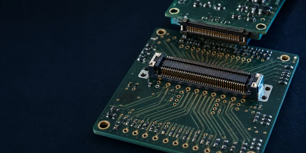
Board-to-board connector failures are often caused by the surrounding PCB and mechanical design rather than the connector itself. A reliable design starts with the released product drawing, then manages stack height, tolerance, footprint geometry, signal return paths, power distribution, mating load, assembly process, and inspection access as one system.
Key Takeaways
- Lock the exact mating pair and revision-controlled vendor drawing before footprint release.
- Treat the connector, two PCBs, supports, enclosure, and assembly motion as one mechanical system.
- Route high-speed channels with continuous return paths and validate the connector transition using supplier models when available.
- Complete DFM, inspection, continuity, and worst-case thermal checks before production approval.
Design Review Summary
| Phase | Primary Task | Typical Failure if Missed |
|---|---|---|
| Mechanical definition | Set board spacing and mating direction | Boards cannot fully mate |
| Footprint | Use current vendor land pattern | Opens, bridges, retention problems |
| High-speed routing | Control breakout and return paths | Excess loss, reflection, crosstalk |
| Power routing | Size copper and vias | Temperature rise and voltage drop |
| Assembly | Validate stencil/reflow/placement | Poor solder yield |
| Verification | Inspect and test the mated assembly | Latent production defects |
1. Start With the Product Drawing
Do not create a generic footprint from pitch alone. The manufacturer drawing defines:
- pad length and width;
- anchor or hold-down pads;
- locating peg holes;
- solder-mask constraints;
- connector origin and datum;
- keep-out zones;
- mating height;
- allowable board-to-board offset;
- recommended PCB thickness where relevant.
Also verify document revision. A family can contain multiple shell, latch, orientation, or stack-height variants with different PCB geometry.
2. Build the Mechanical Tolerance Stack
For mezzanine and coplanar B2B designs, calculate worst-case relative connector position using:
- PCB outline tolerance;
- component placement tolerance;
- connector housing tolerance;
- standoff or chassis tolerance;
- board bow/twist;
- thermal expansion;
- connector self-alignment or floating range.
The key question is not “does it fit at nominal?” but “will every production unit mate without excessive force at worst-case tolerance?”
3. Define Keep-Out Zones in 3D
A connector keep-out is more than a rectangle around the footprint. It should cover:
- mating approach path;
- latch or release motion;
- floating travel;
- tool access;
- rework nozzle access;
- board separation angle;
- opposing-board component height.
Use the connector STEP model when available and place both mated PCBs in the mechanical CAD assembly before release.
4. High-Speed Signal Routing
Board-to-board connectors can become a major discontinuity in PCIe, USB, Ethernet, SerDes, MIPI, or other high-speed channels.
Route for the actual interface
Do not apply one impedance value to every differential link. Typical interfaces may use different differential targets, and the PCB stack-up and connector model must be considered together.
General practices include:
- maintain continuous reference planes through the breakout;
- keep differential-pair geometry symmetric;
- minimize unnecessary layer changes;
- place return vias near reference-plane transitions;
- avoid long via stubs at high data rates;
- follow the supplier’s recommended pin assignment if provided;
- include the connector’s S-parameters in channel simulation when the data rate warrants it.
At advanced data rates, connector performance should be validated in the full channel rather than judged from pitch or marketing bandwidth alone.
5. Power and Ground Routing
Power contacts need low-resistance copper paths on both boards. Check:
- total current and peak current;
- number of parallel contacts;
- current-sharing symmetry;
- plane/trace cross-section;
- via arrays;
- connector pad thermal spreading;
- allowable voltage drop;
- local airflow and ambient temperature.
Avoid routing several high-current connector pads through one narrow copper bottleneck. In high-power designs, the PCB transition can be more resistive than the connector contact.
6. Ground Allocation and Return Paths
Ground pins are not only “extra pins.” They provide:
- power return current;
- high-speed reference continuity;
- crosstalk control;
- ESD/current return paths;
- common-mode containment.
Pin count should therefore be planned from the actual interface topology. High-speed connectors with open pin fields often allow different signal/ground patterns; use field-solver or S-parameter data when necessary rather than applying a fixed ground-to-signal ratio.
7. SMT Assembly and Reflow
For SMT board-to-board connectors:
- use the recommended land pattern;
- verify paste aperture with the EMS provider;
- control board warpage;
- select a placement nozzle compatible with the connector body;
- confirm reflow profile against the connector specification;
- ensure metal hold-downs receive sufficient solder volume;
- inspect first-article assemblies before volume build.
Fine-pitch connectors are particularly sensitive to solder-mask registration, paste volume, and coplanarity.
8. Inspection and Test
Use the inspection method that can actually see the defect mode.
| Method | Useful For |
|---|---|
| AOI | Visible leads, component position, solder fillets |
| X-ray | Hidden joints or structures not optically accessible |
| Continuity / ICT | Opens and shorts |
| Functional test | Interface operation under realistic conditions |
| Mating-force check | Misalignment, damaged contacts, incorrect parts |
| Thermal test | Power-contact temperature rise |
A first-article mating fixture is useful for wide connectors because it controls insertion direction and reduces board damage during process validation.
9. Common Design Mistakes
- assuming nominal stack height without tolerance analysis;
- copying a footprint from a “similar” connector;
- placing components inside the connector mating envelope;
- breaking the high-speed return path at the connector breakout;
- paralleling power contacts without current-sharing analysis;
- ignoring board flex during mating;
- selecting a connector before confirming EMS process capability;
- omitting access for inspection and rework.
10. Release Checklist
- Mating pair and part numbers verified.
- Correct drawing revision stored with the PCB library.
- Mated height confirmed in 3D CAD.
- PCB land pattern independently reviewed.
- Signal-integrity review completed where required.
- Power-temperature-rise review completed where required.
- Assembly house approved stencil/process assumptions.
- Prototype mating and inspection plan defined.
GSCONN Engineering Support
GSCONN provides connector selection and technical-resource access through its website. For PCB integration, request the applicable drawing, 3D model, datasheet, and high-speed data when available, then base the PCB footprint and simulation on those released files rather than generic dimensions.
FAQ
How much keep-out should I leave around a B2B connector?
There is no universal number. Use the product drawing, mating path, tool access, floating travel, and nearby component envelope to define it.
How many PCB layers are required for a high-speed B2B connector?
Layer count depends on interface speed, breakout density, stack-up, power planes, and routing constraints. A fixed “PCIe Gen4 equals eight layers” rule is not reliable.
Should I use X-ray for every fine-pitch connector?
Only when the joint geometry or inspection plan requires it. Visible SMT terminations may be effectively inspected by AOI; hidden structures may need X-ray.
Related reading:
- SMT Board-to-Board Connector Guide
- High-Density Board-to-Board Connector Guide
- High-Current Board-to-Board Power Connector Guide
Technical References
- IPC printed-board design standards overview
- IPC-2152 current-carrying-capacity standard
- Molex SlimStack hardware interface guide
Related reading on GSConn
- Wire-to-Board vs Board-to-Board Connectors
- Industrial USB Connector Guide
- IP67 vs IP68 USB Connector
- Stacked USB Connector Guide
- Request a Quote
Engineering references
- Product drawing, datasheet, material declaration and qualification report for the selected connector series
- IPC land-pattern and acceptability guidance applicable to the PCB assembly class
- Project-specific vibration, shock, thermal and electrical requirements