
USB Connector Signal Integrity and Performance Specifications
Signal integrity is the difference between a USB connector that transmits data reliably at 10 Gbps and one that produces intermittent errors, dropped packets, and failed enumeration. At USB 2.0 speeds (480 Mbps), almost any connector works — the signal is slow enough that impedance mismatches and crosstalk have minimal impact. At USB 3.2 Gen 2 (10 Gbps) and USB4 (40 Gbps), the connector becomes a critical signal integrity element, and the specifications that determine performance are not the ones highlighted in a consumer product listing.
This reference covers the electrical performance specifications that matter for USB connectors at SuperSpeed data rates, how to interpret them on a datasheet, and how connector design choices affect signal integrity.
Why Signal Integrity Matters at High Speed
A 10 Gbps USB 3.2 Gen 2 signal has a fundamental frequency of 5 GHz. At this frequency:
- A 1mm trace length mismatch between differential pair legs creates 5.7ps of skew, which converts 15% of the differential signal energy into common-mode energy — energy that doesn’t carry data and contributes to EMI.
- A 0.5mm discontinuity in the signal path (via, connector transition, pad) creates a reflection that distorts the signal eye diagram.
- Crosstalk between adjacent differential pairs in a stacked connector can couple enough energy to cause bit errors if the pairs aren’t adequately shielded.
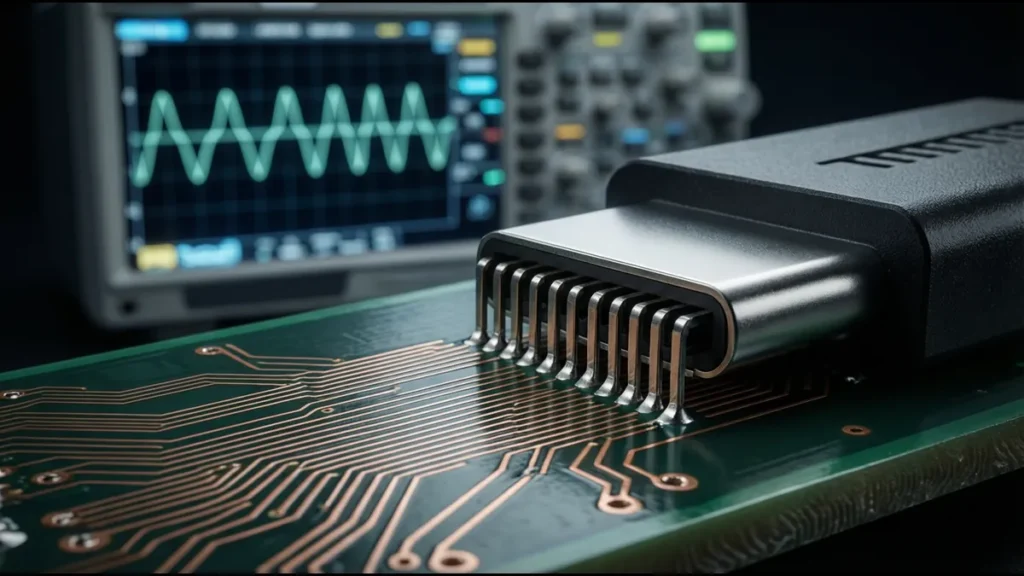
The USB connector is a transition point between the PCB and the cable. This transition — where signals leave the controlled-impedance PCB environment and enter the cable — is where most signal integrity degradation occurs. A well-designed connector makes this transition transparent; a poorly designed one introduces reflections, attenuation, and crosstalk that limit the maximum data rate.
Differential Impedance
What It Is
USB SuperSpeed signals use differential signaling — two conductors carry complementary versions of the same signal. The differential impedance is the impedance between the two conductors of the pair (not to ground). USB 3.x and USB4 require 90Ω ±10% differential impedance (81–99Ω).
Why USB Uses 90Ω, Not 100Ω
Most high-speed differential standards (Ethernet, PCIe, HDMI) use 100Ω differential impedance. USB uses 90Ω for historical reasons — the original USB 2.0 specification was designed with 90Ω differential impedance, and this was carried forward to SuperSpeed to maintain backward compatibility in connector and cable design.
This means you cannot use “standard” 100Ω USB-C cables for Ethernet or PCIe applications without an impedance transformation. USB-C Alt Mode cables that support Thunderbolt/PCIe handle this internally, but for PCB design, the USB traces must be 90Ω, not 100Ω.
Connector Contribution to Impedance
The USB connector introduces an impedance discontinuity at the transition from PCB to cable. Inside the connector, the contact geometry (contact beam width, spacing, and length) determines the local impedance. A well-designed USB-C connector maintains 90Ω ±15Ω through the contact region. A poorly designed one may drop to 60–70Ω or rise to 120Ω, creating a reflection point.
| Connector Quality | Impedance Range Through Connector | Reflection (Return Loss) | Data Rate Impact |
|---|---|---|---|
| Premium (USB-IF certified) | 81–99Ω | ≤ −10dB at 5GHz | Negligible — supports 40 Gbps |
| Standard (compliant) | 75–105Ω | ≤ −8dB at 5GHz | Minor — supports 10 Gbps |
| Low-cost (non-certified) | 60–120Ω | −3 to −6dB at 5GHz | Significant — may fail at 5 Gbps |
Measuring Connector Impedance
Connector impedance is measured using a Time Domain Reflectometer (TDR). A TDR sends a fast rise-time pulse down the signal path and measures reflections. The reflection amplitude and timing reveal the impedance at each point along the path.
A TDR plot of a good USB-C connector shows:
- Flat 90Ω region on the PCB trace
- Brief dip or rise (±10Ω) at the connector contact region
- Return to 90Ω in the cable
A TDR plot of a poor connector shows:
- Large impedance excursion (±30Ω or more) at the contact region
- Multiple excursions indicating multiple discontinuity points
- Ringing or oscillation indicating resonant structures
Insertion Loss
What It Is
Insertion loss is the attenuation of the signal as it passes through the connector. It’s measured in decibels (dB) — a more negative number means more loss. USB-IF specifies maximum insertion loss for USB-C connectors:
| Frequency | USB 3.2 Gen 1 (5 Gbps) | USB 3.2 Gen 2 (10 Gbps) | USB4 (20 Gbps) | USB4 (40 Gbps) |
|---|---|---|---|---|
| 0.1–1 GHz | ≤ −0.6 dB | ≤ −0.6 dB | ≤ −0.6 dB | ≤ −0.5 dB |
| 1–2.5 GHz | ≤ −0.7 dB | ≤ −0.7 dB | ≤ −0.7 dB | ≤ −0.6 dB |
| 2.5–5 GHz | ≤ −1.0 dB | ≤ −1.0 dB | ≤ −1.0 dB | ≤ −0.8 dB |
| 5–10 GHz | — | ≤ −1.5 dB | ≤ −1.5 dB | ≤ −1.2 dB |
| 10–20 GHz | — | — | ≤ −2.0 dB | ≤ −1.8 dB |
What Causes Insertion Loss in a Connector
- Contact resistance: The DC resistance of the contact interface. For a gold-plated contact with proper normal force, this is 10–30mΩ. At high frequencies, the current flows only on the surface (skin effect), so the AC resistance is higher than the DC resistance. At 5 GHz, the skin depth in gold is approximately 0.11µm — thinner than typical gold plating, meaning current flows entirely in the gold layer.
- Dielectric loss: The insulating material between the differential pair conductors absorbs energy from the signal. The loss tangent (dissipation factor, tan δ) of the connector housing material determines this:
– LCP: tan δ = 0.002–0.006 at 1 GHz (low loss, good for high-speed)
– PBT: tan δ = 0.006–0.012 at 1 GHz (moderate loss, adequate for 5 Gbps)
– PPS: tan δ = 0.001–0.003 at 1 GHz (very low loss, excellent for high-speed)
- Radiation loss: At discontinuities (bends, transitions, impedance mismatches), some signal energy radiates rather than continuing down the transmission line. This is usually small but contributes to EMI.
Material Impact on Insertion Loss
| Housing Material | tan δ (1 GHz) | Insertion Loss Impact | Recommended Max Data Rate |
|---|---|---|---|
| LCP | 0.002–0.006 | Minimal | 40 Gbps (USB4) |
| PPS | 0.001–0.003 | Minimal | 40 Gbps (USB4) |
| PBT | 0.006–0.012 | Moderate | 10 Gbps (USB 3.2 Gen 2) |
| PA66 | 0.014–0.020 | Significant | 5 Gbps (USB 3.2 Gen 1) |
For USB4 (20–40 Gbps), LCP or PPS housing is effectively mandatory. PBT may work at 10 Gbps but introduces margin loss that can cause failures in marginal designs.
Return Loss
What It Is
Return loss measures the signal energy reflected back toward the source due to impedance mismatches. It’s also measured in dB — a more negative number means less reflection (better). USB-IF return loss limits:
| Frequency | USB 3.2 Gen 1 | USB 3.2 Gen 2 | USB4 |
|---|---|---|---|
| 0.1–1 GHz | ≤ −8 dB | ≤ −10 dB | ≤ −12 dB |
| 1–5 GHz | ≤ −8 dB | ≤ −10 dB | ≤ −12 dB |
| 5–10 GHz | — | ≤ −10 dB | ≤ −12 dB |
| 10–20 GHz | — | — | ≤ −10 dB |
What Causes Return Loss in a Connector
- Impedance discontinuity at contact transition: The contact beam has different geometry than the PCB trace and cable. This creates a local impedance change that reflects signal energy.
- Via transitions: If the connector has through-hole contacts that pass through the PCB, the via barrels create capacitive discontinuities. Surface-mount contacts avoid this but have their own transition challenges.
- Pad capacitance: The solder pads where the connector contacts attach to the PCB add capacitance, lowering the local impedance. This is controlled by minimizing pad size and using anti-pad (clearance) geometry on inner layers.
Design Techniques to Minimize Return Loss
- Co-planar waveguide routing: Route SuperSpeed traces as co-planar waveguides (ground copper on both sides of the signal pair) rather than microstrip. This provides better impedance control at the connector transition.
- Pad optimization: Minimize connector solder pad size. Use non-functional pad removal on inner layers (don’t connect the via/pad to inner-layer copper unless needed).
- Pre-launch routing: Add a short (0.5–1mm) impedance-compensating trace section between the connector pad and the main routing. This section has slightly different width to compensate for the pad capacitance.
- Ground pad geometry: Ensure the ground pads adjacent to the signal pads are the right size to maintain 90Ω through the pad region.
Crosstalk
What It Is
Crosstalk is the coupling of signal energy from one differential pair to another. In a USB connector, the primary crosstalk concern is between the TX and RX pairs — the transmit signal coupling into the receive signal causes self-interference.
Types of Crosstalk
| Type | Description | Impact |
|---|---|---|
| Near-end crosstalk (NEXT) | Coupling measured at the source end of the disturbing pair | Strongest, because the source signal is at full amplitude |
| Far-end crosstalk (FEXT) | Coupling measured at the far end of the disturbed pair | Weaker, because the disturbing signal is attenuated by the time it reaches the far end |
For USB connectors, NEXT is the primary concern because the TX and RX pairs are in close proximity inside the connector.
USB-IF Crosstalk Limits
| Parameter | USB 3.2 Gen 1 | USB 3.2 Gen 2 | USB4 |
|---|---|---|---|
| TX-to-RX NEXT | ≤ −25 dB (0.1–5 GHz) | ≤ −30 dB (0.1–5 GHz) | ≤ −35 dB (0.1–10 GHz) |
| TX-to-RX FEXT | ≤ −30 dB (0.1–5 GHz) | ≤ −35 dB (0.1–5 GHz) | ≤ −40 dB (0.1–10 GHz) |
Connector Design for Crosstalk Control
- Ground shielding between pairs: Inside the connector, a ground structure (metal shield or conductive plastic partition) separates the TX and RX contact pairs. This is the most effective crosstalk mitigation technique.
- Pair spacing: Maximizing the physical distance between TX and RX pairs reduces capacitive and inductive coupling. In a USB-C connector, the TX and RX pairs are on opposite sides of the connector, separated by the VBUS and GND pins.
- Orthogonal routing: If TX and RX pairs must cross, route them at 90° angles on different PCB layers to minimize coupling area.
Stacked Connector Crosstalk
In stacked USB connectors (two ports in a vertical stack), crosstalk between the upper and lower ports is a concern. The two ports share the same connector body, and the contact pairs of the upper port are directly above those of the lower port.
Mitigation techniques:
- Internal ground shield: A metal partition between the upper and lower contact cavities
- Staggered contact arrangement: Offset the upper port contacts so they don’t align with the lower port contacts
- Ground contacts between signal contacts: Use the GND pins (A1, A12, B1, B12) as shielding between SuperSpeed pairs
A stacked connector without internal shielding may have 20dB worse crosstalk than a single connector — enough to cause bit errors at 10 Gbps.
Eye Diagram and Jitter
What Is an Eye Diagram
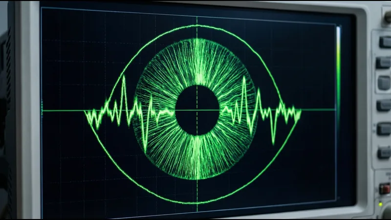
An eye diagram is an oscilloscope display where the received signal is overlaid on itself, synchronized to the clock. The resulting pattern looks like an eye — the open area represents the margin for correctly detecting the signal.
Key Eye Diagram Parameters
| Parameter | What It Measures | USB 3.2 Gen 2 Limit | USB4 Limit |
|---|---|---|---|
| Eye height | Signal amplitude margin | ≥ 70 mV | ≥ 50 mV |
| Eye width | Timing margin | ≥ 0.3 UI (Unit Interval) | ≥ 0.2 UI |
| Jitter (RJ+DJ) | Total timing uncertainty | ≤ 0.3 UIpp | ≤ 0.3 UIpp |
| SNR | Signal-to-noise ratio | ≥ 15 dB | ≥ 12 dB |
How the Connector Affects the Eye Diagram
The connector degrades the eye diagram through:
- Insertion loss: Reduces eye height (amplitude margin). A connector with −1.5dB insertion loss at 5 GHz reduces the signal amplitude by 16%.
- Return loss: Causes signal reflections that create inter-symbol interference (ISI), reducing both eye height and eye width. Reflections from the connector arrive at the receiver delayed by the round-trip time, overlapping with subsequent bits.
- Crosstalk: Adds noise to the received signal, reducing eye height. TX-to-RX crosstalk is particularly damaging because the TX signal is at full amplitude.
- Jitter: Impedance mismatches and reflections convert data-dependent jitter (DDJ) into timing uncertainty, reducing eye width. The connector itself doesn’t add random jitter (RJ), but it converts signal energy into DDJ through reflections.
Eye Diagram Mask Testing
USB-IF compliance testing includes an eye diagram mask test — the eye diagram must not intrude into a defined mask region. If the connector introduces too much loss, reflection, or crosstalk, the eye will close and intrude into the mask, failing the compliance test.
Contact Resistance
What It Is
Contact resistance is the DC resistance of the contact interface — the resistance between the connector contact and the mating plug contact. For USB connectors, the specification is:
| Parameter | Specification | Test Condition |
|---|---|---|
| Initial contact resistance | ≤ 30 mΩ | Per EIA-364-23, 4-wire Kelvin |
| After mating cycling | ≤ 50 mΩ | After 5,000 cycles (industrial) or 1,500 (consumer) |
| After environmental aging | ≤ 60 mΩ | After 96h damp heat (40°C/93%RH) |
Factors Affecting Contact Resistance
- Normal force: Higher contact force creates a larger contact area, reducing resistance. The relationship is non-linear — doubling the force reduces resistance by approximately 30%, not 50%.
- Contact geometry: A rounded (convex) contact beam creates a smaller but more consistent contact area than a flat beam. Point contacts have higher resistance but better stability than line contacts.
- Plating: Gold plating provides low and stable contact resistance. As gold wears through (from mating cycles), the underlying nickel is exposed, and contact resistance increases and becomes unstable (due to nickel oxide formation).
- Contamination: Dust, oil, and oxidation on contact surfaces increase contact resistance. Sealed connectors (IP65+) prevent contamination but add cost.
Contact Resistance and Power Delivery
For USB PD applications delivering 5A at 5V (25W) or 5A at 20V (100W), contact resistance matters significantly:
| Contact Resistance | Power Dissipation per Contact (at 5A) | Temperature Rise (approximate) |
|---|---|---|
| 10 mΩ | 0.25W | +2°C |
| 30 mΩ | 0.75W | +8°C |
| 50 mΩ | 1.25W | +15°C |
| 100 mΩ | 2.50W | +30°C |
At 50mΩ (the post-cycling limit), each VBUS contact dissipates 1.25W. With four VBUS contacts in parallel, the total is 5W — concentrated in a small area. This is why USB-C connectors need all four VBUS pins connected; with fewer pins, the per-contact dissipation is too high.
Mating Cycle Life
Specifications
| Connector Type | Consumer Spec | Industrial Spec | High-Reliability |
|---|---|---|---|
| USB-A | 1,500 cycles | 5,000 cycles | 10,000 cycles |
| USB-C | 10,000 cycles | 10,000 cycles | 15,000+ cycles |
| Micro-USB | 10,000 cycles | — | — |
USB-C is rated for 10,000 mating cycles by design — significantly more than USB-A. This is achieved through:
- Symmetric contact geometry (no cantilever beam that can fatigue)
- Distributed contact force (multiple contact points per pin)
- Lower insertion force (≤ 20N vs ≤ 35N for USB-A)
What Limits Mating Cycle Life
- Plating wear: Each mating cycle removes approximately 0.001–0.003µ” of gold by friction. A 15µ” gold plating lasts 5,000–15,000 cycles before the gold is worn through. A 0.1µ” flash plating lasts 50–300 cycles.
- Contact beam fatigue: The spring beam that provides normal force fatigues with each cycle. Phosphor bronze maintains force for 10,000+ cycles; brass may lose 30% of initial force after 3,000 cycles.
- Housing wear: The plastic housing that guides the plug into position wears with repeated insertion. Excessive wear causes misalignment between plug and contacts, increasing contact resistance and eventually causing open circuits.
Testing Mating Cycle Life
Mating cycle testing per EIA-364-09:
- Insert and extract at a rate of 500–1,000 cycles per hour
- Measure contact resistance every 1,000 cycles
- Measure insertion/extraction force every 1,000 cycles
- Test continues until contact resistance exceeds specification or mechanical failure occurs
The pass criterion is typically: contact resistance ≤ 50mΩ at the rated cycle count, with no mechanical damage visible under 10× magnification.
Current Rating and Power Handling
VBUS Current Capacity
| USB-C Configuration | VBUS Current | Required Pins | Contact Plating |
|---|---|---|---|
| USB 2.0 default | 500 mA | 4 VBUS pins | Gold flash adequate |
| USB 3.2 default | 900 mA | 4 VBUS pins | Gold flash adequate |
| USB Type-C 1.5A | 1.5 A | 4 VBUS pins | 3µ” gold minimum |
| USB Type-C 3A | 3.0 A | 4 VBUS pins | 10µ” gold minimum |
| USB PD 5A (EPR) | 5.0 A | 4 VBUS pins + EPR cable | 15µ” gold minimum |
Thermal Considerations
At 5A, the four VBUS contacts dissipate a combined 2–5W (depending on contact resistance). The connector body temperature rises proportionally. USB-IF specifies a maximum connector body temperature of 100°C during operation.
If the connector is in a sealed enclosure with no air flow, the temperature rise may exceed this limit. Design considerations:
- Provide ventilation or thermal conduction paths away from the connector
- Use connectors with thicker contact beams (lower resistance, less heat)
- Specify contacts with 15µ” minimum gold (lower contact resistance after cycling)
- Derate current if the connector operates at elevated ambient temperature
EMI Shielding Effectiveness
Why It Matters for USB
USB 3.2 Gen 2 (10 Gbps) has a fundamental frequency of 5 GHz with significant harmonic content up to 15 GHz. At these frequencies, any unshielded or poorly shielded portion of the signal path acts as an antenna, radiating EMI that can:
- Fail FCC/CE emissions testing
- Interfere with wireless (Wi-Fi, Bluetooth, cellular) receivers in the same device
- Couple noise into adjacent circuits
Shielding Specifications
| Parameter | Requirement | Test Standard |
|---|---|---|
| Shielding effectiveness (30–300 MHz) | ≥ 60 dB | EN 55032 |
| Shielding effectiveness (300 MHz – 1 GHz) | ≥ 50 dB | EN 55032 |
| Shielding effectiveness (1–10 GHz) | ≥ 40 dB | EN 55032 |
| Transfer impedance | ≤ 100 mΩ/m at 1 GHz | IEC 62153-4-7 |
Connector Shielding Design
- 360° shell grounding: The connector shell must make continuous 360° contact with the cable shield. Spring fingers or fingerstock on the shell provide this contact. A shell that grounds only through solder tabs provides 10–20dB worse shielding.
- Shell-to-chassis contact: The connector shell must make low-impedance contact with the chassis (device enclosure). This is typically through the panel-mount flange or through grounding tabs that solder to the PCB ground plane, which then connects to the chassis.
- Internal shielding: For USB-C connectors operating at 10 Gbps+, the plastic housing between the contact cavities should have embedded metal shielding or conductive coating to prevent radiation through the housing.
Datasheet Interpretation: What to Look For
A USB connector datasheet that claims “USB 3.2 Gen 2 compatible” should include the following signal integrity data. If any are missing, the claim is unsupported:
| Specification | What to Look For | Red Flag |
|---|---|---|
| Differential impedance | 90Ω ±10% (or ±15% through connector) | “Matched impedance” without a value |
| Insertion loss | S-parameter plot or table vs. frequency | “Low loss” without data |
| Return loss | S-parameter plot or table vs. frequency | Not specified at all |
| Crosstalk (NEXT/FEXT) | dB values at relevant frequencies | Not specified for stacked connectors |
| Contact resistance | mΩ value with test method | “Low contact resistance” without value |
| Mating cycle life | Number with test conditions | “High cycle life” without number |
| Current rating | A per VBUS pin, with temperature rise | “High current” without value |
| Operating temperature | Range with humidity | “Industrial temperature” without range |
| Eye diagram margin | Margin values at target data rate | No eye diagram data |
S-Parameters
The most informative signal integrity data is S-parameters (scattering parameters). A USB connector should provide S-parameter data for:
- Sdd11 (differential return loss): How much differential signal reflects back to the source
- Sdd21 (differential insertion loss): How much differential signal transmits through
- Scc11 (common-mode return loss): How much common-mode signal reflects
- SCD21 (differential-to-common-mode conversion): How much differential signal converts to common-mode (indicates asymmetry)
- Sdd31/41 (far-end crosstalk): Coupling between TX and RX pairs
If the datasheet provides S-parameter plots rather than just tables, the manufacturer has done proper characterization. If only tables are provided, check the frequency points — some manufacturers only specify at 1 GHz, hiding performance degradation at higher frequencies.
Connector Selection by Data Rate
| Target Data Rate | Housing Material | Contact Plating | Internal Shielding | Shell Grounding | Mux Required |
|---|---|---|---|---|---|
| USB 2.0 (480 Mbps) | PBT acceptable | Gold flash acceptable | Not required | Solder tab grounding | No |
| USB 3.2 Gen 1 (5 Gbps) | PBT or LCP | 3µ” gold minimum | Recommended | 360° preferred | Yes |
| USB 3.2 Gen 2 (10 Gbps) | LCP preferred | 10µ” gold minimum | Required | 360° required | Yes |
| USB4 20 Gbps | LCP or PPS | 15µ” gold minimum | Required | 360° + internal | Yes |
| USB4 40 Gbps | LCP or PPS | 15–30µ” gold | Required (enhanced) | 360° + internal + chassis | Yes (low-loss) |
At each step up in data rate, the connector requirements become more demanding and the margin for error decreases. A connector that works at 5 Gbps may fail at 10 Gbps due to excess insertion loss, return loss, or crosstalk that wasn’t significant at the lower data rate. Always specify the connector for the highest data rate the system will support, not just the current requirement.
Related Reading: USB Type-C pinout and wiring guide · USB4 connector selection guide · stacked USB PCB layout and signal integrity · DIP vs SMT stacked USB connector · industrial USB connector guide