
DIP vs SMT Stacked USB Connector: Mounting Type Comparison
DIP vs SMT Stacked USB Connector: Mounting Type Comparison
One of the first questions after you choose a USB standard for your stacked connector: through-hole (DIP) or surface-mount (SMT)? There’s no universally right answer — it depends on your assembly process, mechanical environment, and whether the connector is user-facing or internal.
Here’s how the two mounting types compare and when each one makes sense.
Quick Comparison
| Factor | DIP (Through-Hole) | SMT (Surface Mount) |
|---|---|---|
| Mechanical strength | High — pins go through PCB | Lower — pads on surface only |
| Assembly process | Wave or selective soldering | Reflow soldering |
| PCB space (bottom side) | Consumed by pin protrusion | Clean, no protrusions |
| Solder joint inspection | Manual or AOI (difficult) | AOI (easy, visible from top) |
| Rework difficulty | High | Moderate |
| Cost per placement | Higher (wave solder step) | Lower (inline with SMT line) |
| Vibration resistance | Excellent | Requires mechanical anchoring |
| Panel mount compatibility | Natural DIP pins anchor well | Needs additional screws/tabs |
| High-speed signal quality | Via stub effects at GHz | Shorter transition, potentially cleaner |
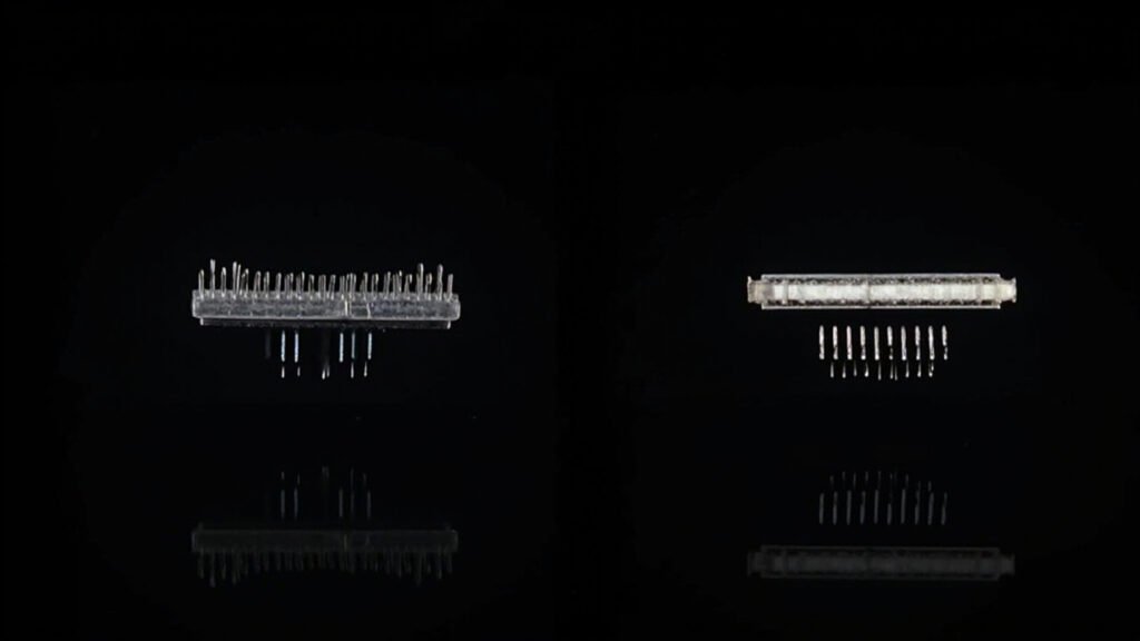
DIP Stacked USB Connectors: When Through-Hole Wins
The Case for DIP
Through-hole mounted stacked USB connectors have pins that go all the way through the PCB and are soldered on the opposite side. This creates a mechanical joint that’s substantially stronger than a surface-mount solder fillet.
Why this matters: A stacked USB connector is tall — typically 14–20mm above the PCB surface. When a user plugs in a USB cable, the insertion force creates a lever arm that tries to peel the connector off the board. A DIP connector’s through-hole pins resist this peeling force much better than SMT pads.
Best applications for DIP:
- User-facing ports subject to frequent cable insertion/removal
- Panel-mounted connectors where the panel provides additional mechanical support
- Products subject to vibration (factory floor equipment, vehicles, outdoor installations)
- Prototype and low-volume builds where hand soldering or manual rework is expected
- Boards that will go through wave soldering anyway (mixed SMT/through-hole designs)
DIP Design Considerations
Pin length: Standard DIP pins protrude 2.0–3.5mm below the PCB. If your board sits in an enclosure with a metal backplane or mounting plate, make sure there’s clearance for the pin tails. A short circuit from a DIP pin tail to a grounded enclosure is surprisingly common in first-revision prototypes.
Wave soldering: Stacked USB connectors have a large plastic body that acts as a thermal shield during wave soldering. The solder wave needs to reach all the pins through the connector body’s shadow. For connectors with 18 pins (USB 3.0 stacked), the inner row of pins may not get adequate solder flow if the wave height or preheat is insufficient. Selective soldering or a second wave pass may be needed.
Via stubs and high-speed signals: For USB 3.0 and above, the unused portion of a through-hole via below the signal layer creates a capacitive stub. At 2.5 GHz (USB 3.0) and above, this stub can create a resonant null. If your SuperSpeed traces are on an inner layer, the via stub length is the distance from that layer to the bottom of the board. On a standard 1.6mm board with the signal layer at mid-board, the stub is ~0.8mm — usually manageable at 5 Gbps but potentially problematic at 10 Gbps. Back-drilling the vias is the fix, but it adds cost.
SMT Stacked USB Connectors: When Surface Mount Wins
The Case for SMT
Surface-mount stacked USB connectors are placed and soldered during the standard reflow process — no separate wave or selective soldering step. For high-volume production, this is a significant cost and throughput advantage.
Best applications for SMT:
- High-volume consumer electronics where assembly cost matters more than mechanical margin
- Internal-only ports that users don’t access directly
- Boards with few or no other through-hole components (all-SMT assembly flow)
- Designs where bottom-side clearance is critical (thin enclosures, no protrusions allowed)
SMT Design Considerations
Mechanical anchoring is mandatory. An SMT stacked USB connector without mechanical anchoring relies entirely on solder fillets to resist the insertion/withdrawal force. For a stacked connector that’s 18mm tall with a 15mm lever arm, a 35N insertion force creates approximately 0.5 N·m of torque at the solder joints. SMT solder fillets alone will not survive this for the rated 1,500+ cycles.
Three common mechanical anchoring methods:
1. Through-hole locating pins (plastic): Two plastic pins on the connector base snap into holes in the PCB. They don’t carry signal, just provide mechanical registration and some additional resistance to lateral force. Better than nothing, but not sufficient for high-cycle-count ports.
2. Through-hole board lock tabs (metal): Two metal tabs on the connector shell go through slots in the PCB and are wave-soldered or hand-soldered on the bottom side. These provide significantly better mechanical anchoring than plastic pins. This is the recommended minimum for user-facing SMT stacked connectors.
3. Panel-mount screw flanges: The connector includes metal flanges with screw holes that fasten directly to the enclosure panel. The insertion/withdrawal force is transferred to the enclosure, not the PCB solder joints. This is the gold standard for industrial SMT stacked connectors.
Co-planarity tolerance: All SMT contact tails on a stacked connector need to sit within 0.10mm of each other to ensure proper solder joint formation during reflow. A stacked connector has more contact tails (8–48 depending on the USB standard) over a larger physical area than a single-port connector, making co-planarity harder to maintain. If your connector manufacturer doesn’t specify co-planarity tolerance, assume it’s >0.15mm — and budget for higher rework rates.
Reflow profile adjustment: The large plastic body of a stacked connector acts as a heat sink during reflow. You may need to extend the time above liquidus (TAL) by 5–10 seconds compared to the rest of your board to ensure the connector’s SMT pads reach proper soldering temperature. A thermocouple on the connector body during profile development is recommended.
Hybrid Mounting: Getting the Best of Both
Some stacked USB connectors use a hybrid approach: SMT for the signal contacts (clean reflow assembly, no stub issues) plus through-hole board lock tabs or shell grounding tabs that can be wave-soldered in a secondary step.
This gives you:
- Clean SMT reflow for the signal pins
- Through-hole mechanical anchoring for strength
- Often a better ground connection through the through-hole shell tabs
The trade-off is an extra assembly step for the through-hole elements. For high-reliability designs, this is usually worth it.
Decision Framework: DIP vs SMT for Stacked USB
Here’s a practical decision sequence:
“`
1. Is this a user-facing port subject to frequent plugging/unplugging?
└─ Yes → DIP or SMT with metal board locks or panel-mount flanges
└─ No (internal only) → SMT is fine with plastic locating pins
2. Is the product subject to vibration or mechanical shock?
└─ Yes → DIP strongly preferred
└─ No → Either
3. Is your assembly process primarily SMT or mixed?
└─ All-SMT line → SMT with anchoring
└─ Mixed SMT/through-hole → DIP (wave solder step already exists)
4. Do you need bottom-side PCB clearance?
└─ Yes (thin enclosure) → SMT
└─ No → Either
5. Are you running USB 3.0 or above with long (>0.8mm) via stubs?
└─ Yes → Consider SMT (avoids stub), or DIP with back-drilling
└─ No → DIP is fine
“`
Common Pitfalls
Pitfall 1: SMT Stacked Connector Without Board Locks
We see this in first-revision prototypes more often than we should. The connector looks fine on the bench. It passes functional test. Six months later, field returns start coming in — intermittent USB connections, ports that work “if you wiggle the cable just right.” The root cause is the SMT solder joints slowly cracking from repeated insertion force, with no board lock to carry the mechanical load.
Fix: Always specify board locks or panel-mount flanges on SMT stacked connectors that face the user.
Pitfall 2: DIP Wave Soldering Shadows
A stacked USB connector with 18 DIP pins has a dense pin field that the solder wave has to penetrate. The outer row of pins gets good solder coverage. The inner row, shielded by the outer row and the connector body, may get incomplete fill or cold joints. This is invisible to visual inspection because the inner row is hidden.
Fix: Verify inner row solder joints with X-ray inspection on first article. If coverage is poor, adjust wave height, preheat temperature, or switch to selective soldering for the connector.
Pitfall 3: Mixed DIP/SMT on the Same Board Without Process Planning
If you have a DIP stacked connector on an otherwise all-SMT board, you’ve introduced a through-hole soldering step (wave or selective) that wasn’t in your original process plan. This adds cost and complexity that should be accounted for during the design phase, not discovered when the CM sends you the assembly quote.
Fix: If possible, keep mounting types consistent across the board. If you must mix, plan the through-hole step in advance and verify your CM has the capability.
Summary
| If your priority is… | Choose… | With… |
|---|---|---|
| Mechanical robustness | DIP | Standard through-hole pins |
| Assembly efficiency | SMT | Metal board locks or panel-mount flanges |
| High-speed signal quality | SMT | (Cleaner transition, fewer via stubs) |
| Low-volume / prototype | DIP | (Easier hand soldering and rework) |
| Thin enclosure | SMT | (No bottom-side protrusions) |
| Industrial / outdoor | DIP | Stainless steel shell, through-hole anchoring |
The mounting type decision matters as much as the USB standard. A poorly anchored SMT stacked connector will fail mechanically long before its electrical rating expires. And a DIP connector on an all-SMT board adds process cost that should have been caught at the design review.
GSConn’s stacked USB connectors are available in DIP, SMT, and hybrid mounting configurations — with board lock, panel-mount flange, and IP-rated sealing options for industrial applications.