
USB Type-C Connector Pinout and Wiring Diagram: Complete Technical Reference
The USB Type-C connector has 24 pins — more than any previous USB connector. Unlike USB-A and micro-USB, which have a fixed plug orientation, USB-C is reversible: the plug can be inserted either way, and the connector is symmetric. This reversibility is achieved through a clever pin arrangement that duplicates key signals on both halves of the connector.
Understanding the Type-C pinout is essential for anyone designing PCBs with USB-C, manufacturing USB-C cables, or debugging USB-C connection issues. This reference covers every pin, its function, and how the connector handles signal routing in both orientations.
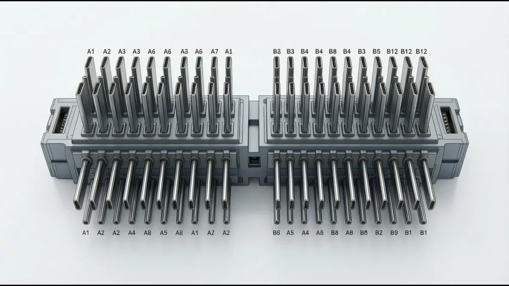
USB Type-C Pin Layout
Receptacle Pin Map (Looking into the Connector)
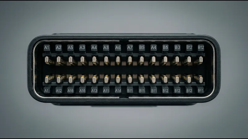
The USB-C receptacle has two rows of 12 pins each. When you look into the receptacle (the port on the device), the pin layout is:
Top row (A1–A12), left to right:
| Position | Pin | Name | Function |
|---|---|---|---|
| 1 | A1 | GND | Ground |
| 2 | A2 | TX1+ | SuperSpeed differential pair 1, positive |
| 3 | A3 | TX1− | SuperSpeed differential pair 1, negative |
| 4 | A4 | VBUS | Power bus (4A capable) |
| 5 | A5 | CC1 | Configuration Channel 1 |
| 6 | A6 | D+ | USB 2.0 differential pair, positive |
| 7 | A7 | D− | USB 2.0 differential pair, negative |
| 8 | A8 | SBU1 | Sideband Use 1 |
| 9 | A9 | VBUS | Power bus (4A capable) |
| 10 | A10 | RX2− | SuperSpeed differential pair 2, negative (receive) |
| 11 | A11 | RX2+ | SuperSpeed differential pair 2, positive (receive) |
| 12 | A12 | GND | Ground |
Bottom row (B12–B1), left to right (note: reversed order):
| Position | Pin | Name | Function |
|---|---|---|---|
| 1 | B12 | GND | Ground |
| 2 | B11 | RX1+ | SuperSpeed differential pair 1, positive (receive) |
| 3 | B10 | RX1− | SuperSpeed differential pair 1, negative (receive) |
| 4 | B9 | VBUS | Power bus |
| 5 | B8 | SBU2 | Sideband Use 2 |
| 6 | B7 | D− | USB 2.0 differential pair, negative |
| 7 | B6 | D+ | USB 2.0 differential pair, positive |
| 8 | B5 | CC2 | Configuration Channel 2 |
| 9 | B4 | VBUS | Power bus |
| 10 | B3 | TX2− | SuperSpeed differential pair 2, negative |
| 11 | B2 | TX2+ | SuperSpeed differential pair 2, positive |
| 12 | B1 | GND | Ground |
Visual Pinout Diagram (Text Representation)
“`
Top Row (A side): A1 A2 A3 A4 A5 A6 A7 A8 A9 A10 A11 A12
│ │ │ │ │ │ │ │ │ │ │ │
GND TX1+ TX1- VBUS CC1 D+ D- SBU1 VBUS RX2- RX2+ GND
│ │ │ │ │ │ │ │ │ │ │ │
Bottom Row (B side): B12 B11 B10 B9 B8 B7 B6 B5 B4 B3 B2 B1
│ │ │ │ │ │ │ │ │ │ │ │
GND RX1+ RX1- VBUS SBU2 D- D+ CC2 VBUS TX2- TX2+ GND
“`
The key observation: the bottom row is a mirror of the top row, but with TX and RX swapped. This mirroring is what makes the connector reversible.
How Reversibility Works
When a USB-C plug is inserted in one orientation, the plug’s A-side contacts connect to the receptacle’s A-side contacts, and the plug’s B-side contacts connect to the receptacle’s B-side contacts.
When the plug is flipped and inserted in the other orientation, the plug’s A-side contacts connect to the receptacle’s B-side contacts, and vice versa.
To handle this, the receptacle has two sets of SuperSpeed differential pairs:
- TX1/RX1 pair: Used when the plug is in orientation 1
- TX2/RX2 pair: Used when the plug is in orientation 2
The device’s USB controller (or a multiplexer chip) detects the plug orientation via the CC pins and routes the SuperSpeed signals to the correct pair. This multiplexing is handled by a “redriver” or “mux” chip in the device — typically integrated into the USB-C controller IC.
USB 2.0 D+/D− Reversibility
USB 2.0 signals (D+ and D−) appear on both rows (A6/A7 and B6/B7). These pins are connected together inside the receptacle — the device simply shorts A6 to B6 and A7 to B7 on the PCB. This means the D+/D− signals reach the USB 2.0 controller regardless of plug orientation, without any switching.
This is possible because USB 2.0 is half-duplex (single direction at a time) and low-speed enough (480 Mbps) that the duplicated pin connection doesn’t cause signal integrity issues. SuperSpeed signals (5 Gbps+) cannot be handled this way — the duplicate connection would cause reflections and signal degradation.
Pin-by-Pin Function Reference
VBUS (A4, A9, B4, B9)
VBUS is the power bus. Four pins carry VBUS to support higher currents:
| USB-C Mode | VBUS Voltage | Max Current | Total Power |
|---|---|---|---|
| USB 2.0 / USB 3.2 (default) | 5V | 900mA (USB 3.2) / 500mA (USB 2.0) | 4.5W / 2.5W |
| USB Type-C Current (1.5A) | 5V | 1.5A | 7.5W |
| USB Type-C Current (3A) | 5V | 3A | 15W |
| USB Power Delivery | 5V–20V | 3A | 15W–60W |
| USB Power Delivery (Extended) | 5V–48V | 5A (with EPR cable) | 100W–240W |
All four VBUS pins must be connected together on the PCB. Using only two VBUS pins (as some low-cost designs do) risks overheating at higher currents — each VBUS pin is rated for approximately 1.5A continuous, so 3A requires all four pins in parallel.
GND (A1, A12, B1, B12)
Four ground pins, symmetrically placed at both ends of both rows. Like VBUS, all four GND pins should be connected together on the PCB. GND pins also serve as the return path for high-speed signals — proper PCB layout requires solid ground planes beneath the signal pairs.
CC1 / CC2 (A5, B5)
The Configuration Channel pins are the most important pins in the USB-C connector. They serve three functions:
1. Plug Orientation Detection
When a plug is inserted, the CC pins on the receptacle detect which orientation the plug is in. Only one CC pin will show a specific voltage (pulled down by the plug’s Rp resistor); the other will be open or at a different voltage. The device’s USB-C controller reads this to determine orientation and configures the SuperSpeed mux accordingly.
2. Current Capability Advertisement
The source (host) advertises its current capability via the CC pin using a pull-up resistor (Rp). The sink (device) detects this resistor value to know how much current it can draw:
| Rp Value (to 1.8V or 3.3V) | Rp Value (current source) | Advertised Current |
|---|---|---|
| 56kΩ | 1.5A (3.3V source) | 500mA (USB 2.0 default) |
| 22kΩ | 330µA (3.3V source) | 1.5A |
| 10kΩ | 180µA (3.3V source) | 3A |
3. USB Power Delivery Communication
When USB PD is supported, the CC pin carries bidirectional BMC (Biphase Mark Coding) data at 600 kbps. This communication negotiates voltage, current, power contracts, and alternate modes. The CC pin is AC-coupled to the PD controller through a 200–300Ω series resistor.
Critical design note: In a captive cable (cable permanently attached to the source), only one CC pin is connected through the cable. The other CC pin on the receptacle is used for VCONN (powering the electronics in the plug). In a detachable cable, both CC pins are connected to the cable’s CC wire, and VCONN is provided on the CC pin that isn’t being used for orientation detection.
D+ / D− (A6, A7, B6, B7)
USB 2.0 differential pair. These pins carry the standard USB 2.0 signals (low-speed 1.5 Mbps, full-speed 12 Mbps, high-speed 480 Mbps). As noted above, the D+ and D− pins on both rows are connected together on the PCB — no switching is needed.
USB 2.0 is the minimum required signal in a USB-C connector. Even a USB-C connector that only supports USB 2.0 data rates (like the charging-only cables that ship with some phones) must have D+ and D− connected.
TX1+/TX1− and TX2+/TX2− (A2/A3, B2/B3)
SuperSpeed transmit differential pairs. These carry the high-speed data signals (5 Gbps for USB 3.2 Gen 1, 10 Gbps for Gen 2, 20 Gbps for USB4). The “TX” designation refers to the direction from the device to the cable — but since USB-C uses dual simplex (separate TX and RX paths in each direction), the naming can be confusing.
In practice:
- TX1+/TX1− and RX1+/RX1− form one SuperSpeed lane pair
- TX2+/TX2− and RX2+/RX2− form the other SuperSpeed lane pair
- Only one pair is active at a time, determined by plug orientation
RX1+/RX1− and RX2+/RX2− (A10/A11, B10/B11)
SuperSpeed receive differential pairs. These are the receive side of the dual simplex connection. The RX pins on one row correspond to the TX pins on the other row — this crossing is part of the reversibility mechanism.
SBU1 / SBU2 (A8, B8)
Sideband Use pins. These are auxiliary pins used for non-USB signals when an Alternate Mode is active:
| Alternate Mode | SBU Usage |
|---|---|
| DisplayPort | SBU1 = DP AUX+ (AUX channel), SBU2 = DP AUX− |
| HDMI | SBU1 = HDMI HEAC+ (Ethernet/Audio Return), SBU2 = HDMI HEAC− |
| Analog Audio | SBU1 = analog audio (mic or speaker), SBU2 = analog ground |
| Thunderbolt 3/4 | Not used (Thunderbolt uses the SuperSpeed pairs) |
When no Alternate Mode is active, the SBU pins are unused and can be left unconnected (or connected to ground through a 0Ω resistor for EMI purposes).
USB-C Cable Wiring
Full-Featured USB-C Cable
A full-featured USB-C cable (supporting USB 3.2 Gen 2 or USB4) contains these wires:
| Cable Wire | Connected To | Wire Count | Notes |
|---|---|---|---|
| VBUS | A4/A9 ↔ A4/A9 (plug to plug) | 4 (2 per side, paralleled) | 20–22 AWG for 3A, 18–20 AWG for 5A |
| GND | A1/A12 ↔ A1/A12 | 4 (2 per side, paralleled) | Same gauge as VBUS |
| D+/D− | A6/A7 ↔ A6/A7 | 2 (connected on both rows) | 28–30 AWG twisted pair |
| TX1+/TX1− | A2/A3 ↔ A2/A3 | 2 | 26–28 AWG twisted pair, 90Ω differential |
| RX1+/RX1− | B11/B10 ↔ B11/B10 | 2 | Same as TX1 |
| TX2+/TX2− | B2/B3 ↔ B2/B3 | 2 | Same as TX1 |
| RX2+/RX2− | A11/A10 ↔ A11/A10 | 2 | Same as TX1 |
| CC | A5 ↔ A5 | 1 | 28 AWG, single wire |
| SBU1/SBU2 | A8/B8 ↔ A8/B8 | 2 | 28 AWG |
| VCONN | B5 (plug 1) ↔ B5 (plug 2) | 0 | VCONN is provided by the source to the plug’s e-marker chip |
Total: approximately 19 conductors in a full-featured cable. This is why USB-C cables are thicker than USB-A cables despite the connector being smaller.
USB 2.0 Only Cable
A USB 2.0 USB-C cable omits the SuperSpeed pairs:
| Cable Wire | Connected To | Wire Count |
|---|---|---|
| VBUS | A4/A9 ↔ A4/A9 | 4 |
| GND | A1/A12 ↔ A1/A12 | 4 |
| D+/D− | A6/A7 ↔ A6/A7 | 2 |
| CC | A5 ↔ A5 | 1 |
| SBU1/SBU2 | Not connected | 0 |
| VCONN | B5 (for e-marker if >3A) | 1 (from source) |
Total: approximately 11 conductors. These cables are thinner, cheaper, and only support USB 2.0 data (480 Mbps) and USB PD power.
E-Marker Chip
Any USB-C cable that supports more than 3A current (5A, for 100W+ charging) or more than 5V VBUS (for USB PD above 5V) must contain an e-marker chip inside the plug. This chip:
- Stores cable identity, capabilities (max voltage, max current, data rate), and manufacturer info
- Communicates with the source device via the CC line (using USB PD messages)
- Allows the source to verify the cable can handle the requested power before applying it
Without an e-marker chip, a USB-C cable is limited to 3A / 5V = 15W maximum. If a cable claims 100W charging but has no e-marker, it’s non-compliant and potentially dangerous.
PCB Layout Guidelines for USB-C
SuperSpeed Signal Routing
The SuperSpeed differential pairs (TX and RX) require careful PCB layout:
| Parameter | Requirement | Reason |
|---|---|---|
| Differential impedance | 90Ω ±10% | Matched to cable impedance to prevent reflections |
| Single-ended impedance | 45Ω ±10% | Each trace in the pair |
| Trace width | 0.18–0.25mm (4–6 mil) on 0.2mm dielectric | Achieves 90Ω differential on standard 4-layer board |
| Pair spacing | 0.15–0.20mm (4–5 mil) within pair | Tight coupling for noise immunity |
| Pair-to-pair spacing | ≥ 3× trace width | Prevents crosstalk between pairs |
| Length matching | ±5 mil within pair, ±15 mil between pairs | Prevents intra-pair skew and differential-to-common-mode conversion |
| Via count | 0–2 vias per signal path | Vias cause impedance discontinuities |
| Layer transitions | Ground via adjacent to each signal via | Provides return path for high-frequency currents |
The Mux Challenge
Because USB-C has two sets of SuperSpeed pairs and only one set is active at a time, the device needs a multiplexer to route the active pair to the USB controller. This mux can be:
- Integrated in the USB controller: Some SoCs (like Intel Tiger Lake and later) have integrated USB-C muxes. The SuperSpeed pairs from both sides of the connector are routed directly to the SoC, which internally selects the active pair.
- External mux/redriver chip: A separate IC (e.g., TI HD3SS3212, NXP PTN5150) sits between the USB-C connector and the USB controller. The CC controller signals the mux to select the correct pair based on plug orientation.
- No mux (USB 2.0 only): If the device only supports USB 2.0, no mux is needed — D+/D− are connected on both rows and only one set of wires goes to the controller.
For designs supporting USB 3.2 or USB4, an external mux or controller-integrated mux is mandatory. The PCB layout must route both SuperSpeed pairs from the connector to the mux, then a single pair from the mux to the controller.
VBUS and GND Layout
| Guideline | Reason |
|---|---|
| Connect all four VBUS pins together with wide copper pour | Distributes current, reduces inductance, prevents pin overheating |
| Connect all four GND pins together to solid ground plane | Low-impedance return path for all signals |
| VBUS trace width: 1.5mm minimum for 3A, 2.5mm for 5A | Prevents trace heating at rated current |
| Add bulk capacitance on VBUS (10–22µF) | Handles transient current draw |
| Add decoupling on VBUS (0.1µF + 0.01µF) | Filters high-frequency noise |
CC Pin Layout
- Route CC1 and CC2 separately to the USB-C/PD controller
- Add a 200–300Ω series resistor if USB PD is used (AC coupling for BMC signals)
- Add ESD protection on both CC pins (the CC pins are exposed to the outside world through the cable)
- Keep CC traces short (≤ 50mm) to minimize capacitance, which affects PD communication
Common USB-C Pinout Mistakes
1. Not Connecting All VBUS/GND Pins
Mistake: Only connecting two of the four VBUS pins (or two of the four GND pins) to save PCB routing space.
Consequence: The connector may work at low currents (500mA), but at 3A or 5A, the connected pins overheat. The contact resistance of a single VBUS pin is approximately 30mΩ — at 3A, that’s 0.27W per pin. With all four pins sharing the load, each pin dissipates 0.07W. With only two pins, each dissipates 0.14W — manageable but approaching limits. With one pin, 0.27W causes significant heating.
2. Swapping D+ and D−
Mistake: Reversing D+ and D− on the PCB.
Consequence: USB 2.0 devices won’t enumerate. The USB controller sees the wrong polarity and can’t decode the differential signal. This is the most common PCB layout error in USB-C designs.
3. Not Handling the Mux
Mistake: Routing only one set of SuperSpeed pairs (e.g., TX1/RX1) to the USB controller and leaving the other set unconnected.
Consequence: The device only works when the plug is in one orientation. When flipped, no SuperSpeed data flows. USB 2.0 still works (because D+/D− are duplicated), but the user sees USB 2.0 speeds half the time they plug in.
4. Wrong CC Pin Resistor Values
Mistake: Using fixed 56kΩ pull-up resistors on CC1 and CC2 (the old USB Type-C 1.0 default) instead of a proper CC controller.
Consequence: The device advertises only 500mA current capability, even if the power supply can deliver 3A. Devices charge slowly or not at all. Additionally, with fixed resistors, USB PD negotiation is impossible — the device can’t request higher voltages.
5. Leaving SBU Pins Floating
Mistake: Not connecting SBU1 and SBU2 to anything.
Consequence: For USB-only operation, this is fine. But if an Alternate Mode (DisplayPort, HDMI) is needed later, the SBU signals have no path. Best practice: route SBU pins to a test point or header, even if initially unused.
6. No ESD Protection on Exposed Pins
Mistake: Not adding ESD protection diodes on VBUS, CC, D+/D−, and SBU pins.
Consequence: USB-C connectors are frequently exposed to ESD events during plug insertion. Without protection, the USB controller or SoC can be damaged. ESD protection diodes (e.g., TVS diodes rated for IEC 61000-4-2 Level 4) should be placed as close to the connector as possible.
USB-C vs USB-A Pinout Comparison
| Feature | USB-A (4 pin) | USB-C (24 pin) |
|---|---|---|
| Data pins | D+, D− (2 pins) | D+, D− (4 pins, 2 per row) |
| Power pins | VBUS, GND (2 pins) | VBUS × 4, GND × 4 (8 pins) |
| SuperSpeed | None | TX1±, RX1±, TX2±, RX2± (8 pins) |
| Configuration | None | CC1, CC2 (2 pins) |
| Sideband | None | SBU1, SBU2 (2 pins) |
| Reversible | No (keyed, one orientation) | Yes (symmetric, either orientation) |
| Max power | 5V, 900mA (USB 3.0) = 4.5W | 48V, 5A = 240W (USB PD EPR) |
| Max data rate | 5 Gbps (USB 3.0) | 40 Gbps (USB4 / Thunderbolt 4) |
| Alt Mode support | None | DisplayPort, HDMI, Thunderbolt, analog audio |
The USB-C connector packs 6× the pin count of USB-A into a smaller form factor. This density is why PCB layout for USB-C is significantly more complex and why the connector requires active components (CC controller, mux) that USB-A does not.
Debugging USB-C Connection Issues
Device Doesn’t Enumerate (No Data)
| Check | Likely Cause |
|---|---|
| D+/D− continuity from connector to controller | Broken trace, wrong pin mapping |
| CC pin resistor/controller configuration | No CC pull-up → device thinks nothing is connected |
| VBUS present at connector | Power not reaching connector |
| Plug orientation (try flipping) | Mux not configured, or only one set of SuperSpeed pairs routed |
Device Enumerates at USB 2.0 Speeds Only
| Check | Likely Cause |
|---|---|
| SuperSpeed pair continuity | Broken TX or RX trace |
| Mux configuration | Mux not switching, or controller not detecting orientation |
| Plug orientation (try flipping) | Only one set of SuperSpeed pairs connected |
| Cable type | USB 2.0-only cable (no SuperSpeed wires) |
Device Doesn’t Charge or Charges Slowly
| Check | Likely Cause |
|---|---|
| CC resistor values | Wrong Rp value → low current advertisement |
| VBUS pin count | Missing VBUS connections → high resistance, voltage drop |
| Cable e-marker | Non-compliant cable without e-marker → limited to 3A/5V |
| PD controller | No USB PD negotiation → stuck at 5V default |
Intermittent Connection
| Check | Likely Cause |
|---|---|
| Connector solder joints | Cold solder, cracked joint from mechanical stress |
| Cable quality | Loose wires inside cable, poor strain relief |
| Connector wear | Worn contacts from high mating cycle count |
| ESD damage | Controller partially damaged by ESD event |
Related Reading: USB connector signal integrity specs · USB4 vs Thunderbolt 4 connector differences · USB4 connector selection guide · stacked Type-C connector USB4-ready · stacked USB footprint and pinout