
PCB Terminal Block Soldering: TH, THR and SMT Guide
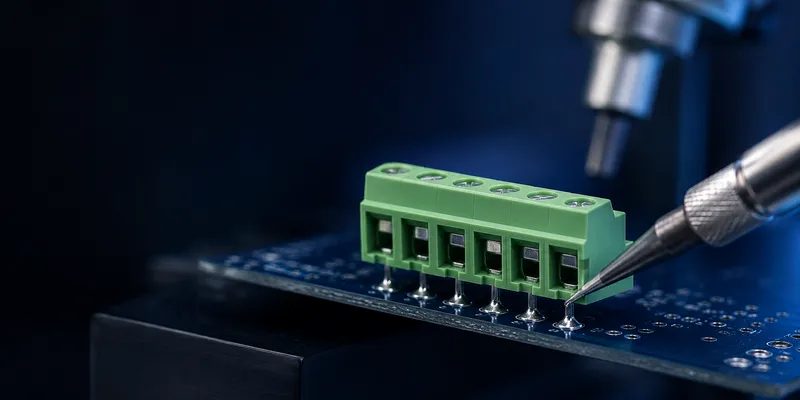
PCB terminal blocks combine an electrical connector with a mechanically loaded board interface. The solder process must create a reliable current path while keeping the housing seated, the pins aligned and the joint strong enough for wire insertion and service loads. This guide compares through-hole, pin-in-paste/THR and surface-mount methods and highlights the process data that should come from the exact component datasheet.
Process Quick Reference
Temperatures and dwell times are representative starting points only. The terminal supplier’s soldering profile and the solder-alloy specification take priority.
| Mounting | Soldering Method | Max Temperature | Notes |
|---|---|---|---|
| Through-hole (TH) | Wave solder or hand-solder | 260°C (3s per pin) | Standard for PCB terminals |
| Through-hole reflow (THR) | SMT reflow in same process | 235–245°C peak (SAC305) | Requires THR-compatible terminal |
| SMT | Reflow oven | 235–245°C peak | PA9T or LCP housing required |
| Press-fit | No solder — mechanical interference | N/A | Requires plated through-holes, special pin design |
1. Through-Hole PCB Terminal: The Standard
Most PCB terminal blocks use through-hole mounting with square pins (0.6–1.0mm) soldered into plated holes.
Solder Process Options
| Process | Equipment | Best For |
|---|---|---|
| Wave soldering | Wave solder machine | High-volume production, single-sided PCB |
| Hand soldering | Soldering iron (60W+) | Prototypes, low volume, repair |
| Selective soldering | Robotic soldering | Mixed TH/SMT boards, bottom-side only |
Hand-Soldering Procedure
- Insert terminal block into PCB — ensure it sits flush
- Tack-solder one end pin to anchor the terminal
- Solder the remaining pins using the component’s specified tip temperature and dwell time; a common manual starting point is about 350°C for 2–3 seconds per pin
- Inspect wetting, fillet shape and hole fill against the applicable workmanship standard; lead-free joints are not always mirror-shiny
- No solder bridging between adjacent pins (critical for fine pitches like 3.5mm)
Common Issues
| Issue | Cause | Solution |
|---|---|---|
| Terminal lifted off PCB | Too much solder in hole before insertion | Insert terminal first, then solder |
| Poor wetting or disturbed joint | Oxidation, insufficient heat, contamination or movement during cooling | Correct the process cause, then rework with compatible flux and controlled heat |
| Housing melted | Iron too hot or dwelled >5 seconds | 350°C max, 2–3 seconds per pin, let cool between pins |
| Bridging (3.5mm pitch) | Excess solder, large tip | Use fine conical tip (0.8mm), less solder |
2. Through-Hole Reflow (THR): SMT + TH in One Pass
THR terminals are designed to be soldered in the same reflow oven as SMT components. Paste is printed into plated through-holes, the THR terminal pins are inserted, and the entire board goes through reflow.
Requirements
| Parameter | Requirement |
|---|---|
| Terminal housing | Reflow-qualified high-temperature material such as an appropriate LCP or polyamide grade; verify the exact peak profile. Do not assume material family alone proves compatibility. |
| Pin design | Tapered tip for easy insertion into paste-filled holes |
| Paste volume | Calculate for the required barrel fill, pin displacement and acceptable top/bottom fillets; validate by cross-section or process inspection |
| Stencil | Step stencil with thicker paste deposit at THR holes |
Advantages Over Wave Soldering
- One pass for all components (SMT + TH)
- Eliminates separate wave solder step
- Greater freedom for mixed-technology board layouts, subject to component keep-outs and reflow access
3. SMT PCB Terminal Blocks
SMT terminals eliminate through-holes — all pads are on the board surface. Saves PCB layers (no via needed for each pin) and allows components on both sides.
| Parameter | SMT PCB Terminal |
|---|---|
| Pitch | 3.5, 5.0, 5.08mm |
| Housing | PA9T or LCP (reflow-safe) |
| Coplanarity | <0.10mm across all pads |
| Mechanical strength | Lower than TH (no through-hole anchor) |
SMT can simplify double-sided assembly and eliminate plated-through mounting holes, but the board pads and mechanical support must withstand wiring and service loads. Through-hole remains common in industrial equipment because the pins provide additional mechanical anchoring. For large pluggable connectors or high mating forces, consider board locks, flanges or chassis support.
4. Design-for-Soldering Checklist
- Use the recommended hole, pad and stencil dimensions for the exact part number.
- Confirm housing material and packaging are qualified for the intended process.
- Include keep-outs for solder pallets, selective nozzles, reflow shadowing and inspection access.
- Control connector seating and coplanarity before soldering.
- Account for copper planes that draw heat away from individual pins.
- Inspect hole fill, wetting and bridging to the applicable workmanship class.
- Perform pull, torque or mating-force validation when the connector sees significant mechanical load.
- Recheck electrical temperature rise after final solder-process validation.
Common Questions
Can every through-hole terminal block go through reflow?
No. Pin-in-paste/THR requires a housing, pin design and packaging qualified for the reflow profile. A standard wave-solder component may deform or shift.
Is a dull lead-free solder joint defective?
Not necessarily. Judge the joint by wetting, contour, fill, cracks and the applicable inspection criteria—not brightness alone.
Why does one pin show poor hole fill?
Large copper planes, insufficient paste or flux, pin-to-hole mismatch, oxidation and thermal imbalance are common causes. Correct the process window rather than simply increasing heat everywhere.
5. GSConn PCB Terminal Soldering Options
| Series | Mounting | Housing | Max Reflow Temp | Soldering Method |
|---|---|---|---|---|
| TB-SC-350 (3.5mm) | TH | PA66 | N/A (wave only) | Wave or hand solder |
| TB-SC-508-THR (5.08mm) | THR | LCP | 245°C | Reflow or wave |
| TB-SP-508-SMT (5.08mm) | SMT | PA9T | 245°C | Reflow |
Request Process Data Before Release
GSConn PCB terminal families include through-hole, pin-in-paste/THR and SMT options. Request the land pattern, hole recommendation, approved solder profile, packaging and mechanical data for the exact series before the PCB and assembly process are finalized.
Related reading: