
Stacked USB 3.0 Connector: Practical Specification and Selection Guide
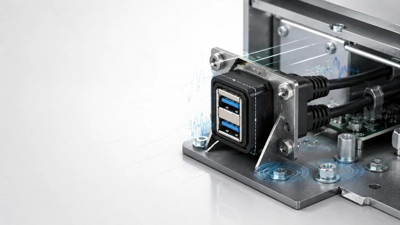
USB 3.0, also marketed in later naming schemes as USB 3.2 Gen 1, runs at 5 Gbps. At that speed, a stacked connector is no longer just a space-saving mechanical part. Its internal geometry, shield structure, grounding, and PCB breakout all become part of the high-speed channel.
This guide explains how to select and lay out a stacked USB 3.0 Type-A connector without over-promising what the connector alone can guarantee.
Quick specification checklist
| Item | What to verify |
|---|---|
| USB speed | 5 Gbps SuperSpeed / USB 3.x Gen 1 support for the selected part. |
| Impedance | 90 Ω differential channel target, including connector breakout. |
| Shielding | Metal shell and clear shell-to-chassis bonding method. |
| Mounting | Through-hole or hybrid mounting for field-accessible ports. |
| Current rating | Connector contact rating and system VBUS limit are not the same thing. |
| Temperature | Commercial, industrial, or extended-temperature version as required. |
| Documentation | Drawing, footprint, 3D model, and SI data where available. |
1. USB 3.0 Type-A pinout in a stacked connector
A USB 3.0 Type-A receptacle has the four USB 2.0 contacts plus five SuperSpeed contacts. In a stacked two-port connector, this set is duplicated for the upper and lower ports.
| Pin group | Signal | Design note |
|---|---|---|
| Power | VBUS, GND | Use current limiting and ESD protection per port. |
| USB 2.0 data | D+, D− | Still required for enumeration and backward compatibility. |
| SuperSpeed RX | SSRX+, SSRX− | Route as a controlled differential pair. |
| SuperSpeed TX | SSTX+, SSTX− | Route as a controlled differential pair. |
| Shield | Connector shell | Bond to chassis or shield ground with low impedance. |
Do not merge the two ports electrically just because they share one housing. Each port needs its own routing, ESD strategy, and VBUS power control.
2. What stacking changes at 5 Gbps
The lower port usually has a shorter path from contacts to PCB. The upper port must route down through the connector body. That internal path can add length and discontinuities, and the two ports sit close enough that port-to-port coupling becomes relevant.
The result is not automatically a failed link. Many shielded stacked USB 3.0 connectors work well at 5 Gbps. The point is that margin is lower than with two well-spaced connectors, so the rest of the channel should be clean.
Practical implications:
- choose a shielded connector for USB 3.x;
- keep the host-to-connector route short;
- avoid unnecessary vias and stubs;
- use the connector vendor’s footprint, not a guessed pattern;
- run pre-compliance testing with the real cable and enclosure.
3. Signal-integrity guidance
For a 5 Gbps USB 3.x link, the entire channel matters: controller package, PCB route, connector, cable, and device. The connector vendor may provide S-parameters or test data, but those do not replace board-level validation.
| Parameter | Practical target |
|---|---|
| Differential impedance | 90 Ω target through route and breakout. |
| Intra-pair skew | Keep small; follow the controller and USB layout guide. |
| Return path | Continuous reference plane under SuperSpeed pairs. |
| Vias | Minimize; add nearby ground return vias when changing layers. |
| ESD capacitance | Use parts suitable for SuperSpeed lines. |
| Stub length | Avoid test pads and unused branch traces on SuperSpeed pairs. |
A common layout error is to route the upper and lower ports symmetrically on the PCB without considering the connector’s internal geometry. Use the supplier footprint and recommended escape routing. If the vendor provides a channel model, include it before committing to a dense four-layer layout.
4. Grounding and shielding
The connector shell should not be treated as an afterthought. For EMC and ESD, the shell needs a low-impedance return path.
Recommended practices:
- Place stitching vias around shell/mounting pads.
- Keep a solid ground reference under the connector breakout.
- Avoid splitting digital ground under the USB pairs.
- Connect the shell to chassis where the mechanical design allows it.
- Use a shielded USB 3.x cable for validation and production recommendations.
If the device uses a plastic enclosure, the shell-bonding strategy needs extra attention. A connector shell tied only to a long, narrow PCB trace is a poor ESD path.
5. Mechanical specifications to check
A stacked connector saves width but increases height. The upper port also applies insertion force farther from the PCB surface, so mechanical support is important.
| Mechanical item | Why it matters |
|---|---|
| Body height | Must fit the enclosure and cable overmold. |
| Panel cutout | Check upper and lower port access, not only connector body size. |
| Shell stakes | Improve retention and reduce solder stress. |
| Bracket option | Useful for frequent insertion or industrial vibration. |
| Mating cycle rating | Use the datasheet rating for the exact part. |
| Rework access | Stacked through-hole parts can be harder to inspect than single ports. |
For industrial or medical equipment, place the connector close to a board mounting point or use a bracket. Do not let the connector sit on a flexible PCB edge unsupported.
6. Power and thermal notes
USB 3.0 default bus power and connector contact rating are related but not identical. A connector may have contacts rated above the USB default current, but the system still needs current limiting, power switching, and thermal validation.
When two bus-powered devices are connected at the same time, check:
- 5 V regulator capacity;
- per-port current limit;
- inrush current during plug-in;
- voltage drop to the connector;
- heating near the upper port during sustained current draw.
For high-current charging or USB Power Delivery designs, stacked vertical connectors may not be the best mechanical choice. Type-C power designs require a much broader system review than the connector footprint.
7. Selection path for GSConn projects
For a GSConn stacked USB 3.0 selection, define these inputs before requesting samples:
- USB Type-A or Type-C;
- vertical stacked or right-angle stacked;
- through-hole, SMT, or panel-mount style;
- commercial, industrial, or extended temperature;
- standard or sealed panel version;
- required documentation: drawing, STEP model, test report, SI data, material declaration.
Ask for the current datasheet and footprint for the exact part number. Do not copy a footprint from a different stacked connector family unless the supplier confirms equivalence.
8. Naming clarification: USB 3.0 and USB 3.2 Gen 1
For most connector-selection discussions:
| Name seen in market | Practical meaning |
|---|---|
| USB 3.0 | 5 Gbps SuperSpeed. |
| USB 3.1 Gen 1 | Also 5 Gbps. |
| USB 3.2 Gen 1 | Also 5 Gbps. |
| USB 3.2 Gen 2 | 10 Gbps; requires more careful channel design. |
| USB4 | Type-C ecosystem; do not treat a USB-A stacked connector as USB4-capable. |
For 10 Gbps and above, stacked connector availability and signal margin become much more part-specific. Ask for test data early.
FAQ
Can I use a USB 2.0 cable in a stacked USB 3.0 port?
Yes. The link will operate at USB 2.0 speed because the SuperSpeed contacts are not used by the USB 2.0 cable.
Does stacking always hurt USB 3.0 performance?
It usually reduces margin compared with two separated ports, but a shielded, well-designed stacked connector can be perfectly suitable at 5 Gbps when the PCB and cable are also controlled.
Is a stacked USB 3.0 Type-A connector suitable for USB4?
No. USB4 is a Type-C-based ecosystem. Use a Type-C solution designed and tested for the required data rate.
Should I compensate the upper port length on the PCB?
Do not blindly add or remove length. Follow the connector vendor’s layout guidance and focus on pair matching, impedance, and a clean return path.