
Board-to-Board Stacking Height: How to Select a Floating Connector
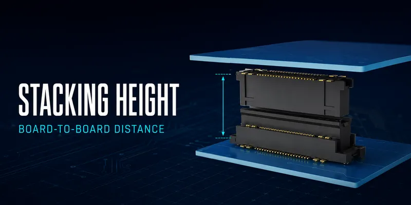
Stacking height—also called mated height or board-to-board distance—is the specified distance between the relevant PCB reference surfaces after a connector pair is fully mated. It is one of the most important mechanical dimensions in a floating B2B design because it directly affects enclosure fit, component clearance, board stiffness, and mating reliability.
The correct value does not come from choosing the closest-looking connector. It comes from a controlled mechanical envelope and the supplier’s drawing.
Quick design inputs
| Input | Why it matters |
|---|---|
| Connector drawing reference surfaces | Defines exactly how mated height is measured |
| PCB thickness and tolerances | Affects enclosure and support-stack dimensions |
| Tallest facing components | Sets the minimum safe internal clearance |
| Board bow, twist, and mounting variation | Determines parallelism and Z tolerance needs |
| Standoff and enclosure geometry | Must carry mechanical loads without overloading the connector |
| Required service and inspection access | May require extra clearance beyond nominal fit |
1. Confirm what the supplier means by “stacking height”
Different documents may reference the top copper surface, PCB surface, component seating plane, or another datum. Start with the connector drawing and identify the two exact surfaces used for the mated-height dimension.
For a parallel-board connector, the key design question is normally: what board-surface-to-board-surface spacing will exist after the boards are mounted in the enclosure? Keep that definition consistent across the mechanical model, PCB drawing, assembly fixture, and incoming inspection plan.
2. Build a component-clearance envelope
The required board spacing must accommodate the tallest opposing components, manufacturing variation, board deflection, and an appropriate clearance reserve.
| Clearance item | Include it? | Notes |
|---|---|---|
| Component height on PCB A facing PCB B | Yes | Use the maximum placement envelope, not typical height. |
| Component height on PCB B facing PCB A | Yes | Check both boards, including solder joints and labels. |
| PCB thickness and flatness | Yes | Use documented fabrication limits. |
| Mechanical tolerance of standoffs/housing | Yes | Include compression, thread, and assembly variation. |
| Electrical clearance | As needed | Consider voltage, pollution degree, and applicable safety rules. |
| Service and airflow gap | As needed | Include probe access, airflow, and thermal requirements. |
Do not select a connector whose nominal mated height is less than the required component envelope. A fixed-height connector cannot safely “make up” missing vertical clearance.
3. Treat Z compliance correctly
Some floating connector families specify limited Z movement or mating compliance. This can help accommodate small parallelism variation during assembly, particularly where several connectors mate between the same boards.
Z compliance is not a substitute for adequate mated height, flat boards, or standoffs. Verify its direction, usable range, force characteristics, and whether it remains available after mating. If the drawing does not explicitly state Z compliance, do not assume it exists.
4. Mechanical support: connectors should not carry the structure
Floating B2B connectors are electrical interconnects with defined retention limits. In a finished product, standoffs, chassis features, screws, guides, or rails should control board position and carry weight, handling force, and external shock loads.
| Design condition | Recommended mechanical feature |
|---|---|
| Two boards in a small fixed enclosure | Standoffs near the connector and at board corners |
| Large or heavy upper board | Multiple supports sized from deflection analysis |
| Blind-mate service module | Lead-in guides and positive seating features |
| Mobile/vibration environment | Controlled supports, retention features, and application-specific test |
| Multiple connectors | Defined board datum and mating sequence to avoid over-constraint |
5. A practical stacking-height workflow
- Create a cross-section. Include both boards, the connector, all facing components, standoffs, enclosure surfaces, shields, and fasteners.
- Assign reference planes. Use the same reference surfaces defined on the connector drawing.
- Calculate the worst-case envelope. Apply component-height, PCB-thickness, mounting, and board-flatness tolerances in the chosen tolerance method.
- Reserve clearance. Add a documented non-contact, electrical, thermal, and service allowance.
- Select available mated height. Choose a product height that meets the calculated requirement while fitting the enclosure.
- Check lateral travel and guides. Correct height does not eliminate the need for X/Y tolerance analysis.
- Build a production-intent sample. Measure board parallelism, actual clearance, mating force, and connector engagement.
6. Common pitfalls
| Pitfall | Consequence | Better approach |
|---|---|---|
| Using enclosure height as the connector height | Board surfaces do not land at the intended distance | Model the complete board and support stack. |
| Measuring from the wrong datum | Incorrect mechanical drawing and fixture | Use the connector drawing’s stated reference surfaces. |
| Ignoring components on the opposing board | Collision after assembly | Create a two-board component envelope. |
| Relying on the connector as a standoff | Stress, incomplete mating, or solder-joint loading | Use dedicated mechanical supports. |
| Choosing nominal height with no tolerance reserve | Interference in production | Stack tolerances and retain documented clearance. |
| Assuming every floating connector has Z travel | Unexpected mating-force or parallelism issue | Confirm Z compliance in the product specification. |
FAQ
Is a 12 mm connector automatically suitable for a 12 mm enclosure gap?
No. Compare board reference surfaces, PCB thickness, standoffs, component envelopes, and all tolerances. Nominal enclosure clearance is not the same as mated height.
Should I select the nearest standard height below my calculated requirement?
No. The selected height must meet the required worst-case clearance. If no standard product does, revise the mechanical architecture or request a suitable qualified option.
Do taller connectors always give better thermal performance?
Not necessarily. More board spacing can improve airflow, but the system result depends on enclosure ventilation, heat sources, shields, and thermal paths.
Request a stacking-height review
Send a mechanical cross-section or 3D model, PCB thicknesses, component keep-out envelopes, required board spacing, number of connectors, desired travel, and environmental requirements. This allows the GSConn engineering team to check mated height, footprint, and support strategy against the exact product drawing.
Related articles: Complete Floating B2B Guide · Float Range Selection · PCB Layout & Assembly · Floating vs Rigid B2B
Related reading on GSConn
Engineering references
- Selected connector mechanical drawing and mating specification
- PCB fabrication drawing and component mechanical models
- Enclosure drawing, support-stack tolerances, and project clearance requirements