
Floating B2B Connector PCB Layout and Assembly Guide
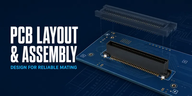
A floating B2B connector can only provide its intended travel and reliability when the PCB footprint, surrounding keep-out, stencil design, placement process, and mechanical support all match the selected part’s documentation. The product drawing is therefore the primary design authority; generic pad sizes should be used only as early planning estimates, never as a release footprint.
Pre-layout checklist
| Document or input | Use it to verify |
|---|---|
| Product drawing | Mated height, land pattern, contact numbering, hold-downs, datum surfaces |
| Recommended PCB footprint | Pads, solder-mask rules, paste apertures, and component courtyard |
| Keep-out/movement drawing | Dynamic clearance around the floating element and mating path |
| Assembly specification | Reflow limits, coplanarity, placement handling, and inspection guidance |
| Signal-integrity data | Pin map, reference-plane needs, and channel constraints |
| Mechanical CAD | Board supports, fasteners, guides, shields, and component envelopes |
1. Use the approved land pattern and dynamic keep-out
Floating designs need more than a static component courtyard. The moving portion of the connector and its mating partner may occupy a larger space during mate or operation. Preserve the supplier’s full keep-out area around the connector body, travel path, keying features, and any service tool access.
Keep nearby components, vias, tall solder joints, screws, heat sinks, shields, labels, and cable features outside this region. A trace that is electrically acceptable may still be mechanically vulnerable if it is inside the dynamic envelope.
Footprint review questions
- Is the footprint taken from the exact part-number drawing and current revision?
- Are all mounting tabs, shield pads, or through-hole retention features included?
- Are solder-mask, paste-mask, and copper clearances consistent with the supplier’s recommendation and your assembler’s design rules?
- Is the connector orientation and pin-1 indication unambiguous in CAD, silkscreen, and assembly drawings?
- Are local fiducials or tooling features needed for the selected pitch and placement process?
2. Plan routing and return paths before filling the area
Assign pins according to the connector supplier’s recommended map, especially where differential pairs, grounds, shields, analog references, or power contacts are involved. Do not assume contact numbering at one end maps visually to the other without checking the mating drawing.
| Routing objective | Good design practice |
|---|---|
| Differential signals | Use the impedance, pair matching, and reference-plane rules of the interface and final stack-up. |
| Return-path continuity | Keep a continuous reference plane and provide return contacts as recommended. |
| Via transitions | Minimize them; maintain symmetry for pair members and control stubs where the channel requires it. |
| Power contacts | Use the specified copper width, thermal relief strategy, and adjacent-contact derating assumptions. |
| Sensitive analog signals | Separate them from switching power and fast edge-rate aggressors. |
When high-speed performance matters, review the connector, PCB, cable, transmitter, and receiver as a single channel. Request S-parameter files and test conditions for the actual connector family where available.
3. Stencil and solder-paste control
The optimum paste type, stencil thickness, and aperture reduction depend on pitch, pad geometry, board finish, solder alloy, and the assembly line. Use the connector supplier’s recommendation, then validate it with the EMS provider on a production-intent coupon or pilot board.
| Process item | What to control |
|---|---|
| Stencil apertures | Paste volume and release for each pad; avoid copying an unrelated connector pattern. |
| Paste alloy and powder size | Compatibility with aperture size and the validated reflow profile. |
| Board support | Prevent board flex during print, placement, and reflow. |
| Placement force | Sufficient seating without damaging the connector mechanism or distorting the board. |
| Reflow | Stay within the connector’s documented temperature/time limits. |
Do not reduce or increase aperture area simply to solve a visual defect without a controlled trial. Paste changes can create open joints, bridging, voids, or flux contamination in a moving interface.
4. Reflow and handling
Verify the housing material and component moisture-sensitivity requirements before defining the profile. The reflow profile must satisfy both the solder alloy and the component specification. If the connector supplier provides a maximum peak temperature, time above liquidus, or preconditioning requirement, those limits take precedence.
Use a supported PCB during reflow to avoid excessive bow or twist. After reflow, handle the board in a way that does not side-load the floating element or drag it across fixtures, trays, or test equipment.
5. Multi-connector assemblies: design the mating operation
When two or more connectors mate between the same board pair, the total insertion force and differential position can become important. Prototype the actual mating operation rather than assuming all connectors will engage simultaneously.
| Check | Why it matters |
|---|---|
| Board supports below/above the connectors | Prevents board bending during mating |
| Guides and datum features | Controls initial approach and rotation |
| Mating direction | Reduces side load and incomplete engagement |
| Total mating force | Determines fixture and operator/automation needs |
| Available travel after mate | Confirms that the connector is not held at its limit |
| Access for inspection/service | Prevents later rework and test difficulties |
6. Inspection and acceptance criteria
Set acceptance criteria with the product drawing, applicable workmanship standard, and your product class. Common checks include:
| Inspection area | Example verification |
|---|---|
| Solder joints | Wetting, bridges, opens, voids, and solder-ball control using the approved method |
| Connector seating | Coplanarity, orientation, hold-down attachment, and no visible lift |
| Moving interface | Free movement within its documented range using the supplier-approved method |
| Mating | Full engagement, keying, latch/retention operation where applicable |
| Electrical | Continuity, isolation, and contact-resistance trend as required |
| Mechanical | No interference with nearby components through the expected travel range |
Do not use metal tools to force the floating element unless the manufacturer explicitly approves that inspection method. A destructive “movement check” can damage contacts or springs.
7. Typical process failures and corrective action
| Symptom | Potential cause | First response |
|---|---|---|
| Solder bridges | Excess paste, stencil alignment, pad/print mismatch | Inspect stencil, paste deposit, and footprint before changing the part. |
| Open or weak joints | Insufficient paste, coplanarity, profile, board support | Review SPI/AOI data and profile against the component limit. |
| Connector tilt or lift | Uneven paste, warped board, placement issue | Check board flatness, placement force, and deposit uniformity. |
| Restricted float | Contamination, mechanical interference, mishandling | Check keep-out and supplier handling guidance; quarantine affected lots. |
| Difficult mating | Incorrect height, positional error, rotation, excessive total force | Measure actual board positions and review mechanical stack-up. |
FAQ
Can I reuse a footprint from a similar-looking connector?
No. Verify every pad, retention feature, keep-out, height, pin map, and mating geometry against the selected part’s current drawing.
Are through-hole retention features always required?
No. Use the configured product’s mounting features and the application loading analysis. Where they are provided, include and solder them as specified.
What is the most important post-reflow check?
Confirm solder integrity, correct seating, and that the moving element is not obstructed—using the supplier-approved method and the product acceptance plan.
Request a layout review
Provide the proposed footprint, PCB stack-up, connector part number, local component placement, signal pin map, reflow profile, and mechanical cross-section. The GSConn engineering team or your EMS partner can review these against the product documentation before the first production build.
Related articles: Complete Floating B2B Guide · Pitch Selection · Float Range Selection · Stacking Height Selection
Related reading on GSConn
Engineering references
- Current product drawing, recommended land pattern, and assembly specification
- Applicable PCB-assembly workmanship and land-pattern standards
- EMS process capability, SPI/AOI data, and product-specific control plan