
How to Select Floating Connector Travel and Tolerance
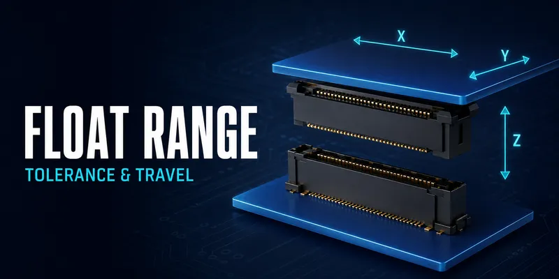
The “float range” of a floating board-to-board connector is the controlled distance its moving interface can travel while remaining within the manufacturer’s specified mating and electrical-performance limits. It is not a universal guarantee that any amount of board movement will be absorbed.
Correct selection starts with an engineering tolerance stack-up. The purpose is to ensure the connector still has usable travel left after the boards are assembled, not merely to make an impressive nominal specification.
Quick selection checklist
| Gather this information | Why it belongs in the calculation |
|---|---|
| Connector positions and count | Determines differential offset between parts |
| PCB datum scheme and fabrication tolerance | Sets the baseline positional uncertainty |
| Placement capability and local fiducials | Determines component-to-datum offset |
| Board dimensions, material, and temperature excursion | Determines thermal movement and potential warp |
| Board supports, enclosure, and assembly sequence | Determines relative motion and parallelism |
| Vibration/shock inputs | Determines operational displacement and test severity |
| Product drawing | Defines the actual travel, mating window, and exclusions |
1. What “float” must compensate for
Lateral X/Y movement is commonly used to absorb relative position error. Some connector families also provide a documented amount of Z compliance, which can help during mating when boards are not perfectly parallel. Product definitions differ, so confirm whether the stated number is per axis, total travel, an offset at first mate, or travel after full engagement.
Potential contributors include:
- PCB feature and board-outline position relative to the mechanical datum
- Pick-and-place accuracy, component coplanarity, and local fiducial quality
- Tolerance between multiple connectors on the same board pair
- Board deflection, bow, and twist after reflow or mounting
- Thermal expansion between different mechanical reference points
- Operational vibration, shock, and enclosure movement
- Rotation and angular error, which create larger offset at connectors far from the datum
2. Use a relative-position stack-up—not a generic rule
For a connector located at a distance from the assembly datum, calculate the relative position of the two mating halves. Include both translation and rotation. A simplified first-pass model is:
ΔXY = ΔPCB + Δplacement + Δmounting + Δthermal + Δdynamic
For production release, use your quality team’s method—such as worst-case, RSS, or a Monte Carlo model—according to the risk and distribution assumptions. Do not add unrelated maximum values and call the result a statistically valid prediction.
Then select a connector whose allowable operating displacement exceeds the approved relative offset plus a mating margin. The margin must account for lead-in geometry, measurement uncertainty, and future process drift.
3. Thermal expansion: calculate it from the mechanical reference
For a first estimate, in-plane expansion is:
ΔL = α × L × ΔT
where $\alpha$ is the in-plane coefficient of thermal expansion, $L$ is the distance from the controlling datum, and $\Delta T$ is the relevant temperature change. FR-4 values vary with construction and temperature; use the laminate data for the final calculation.
Thermal expansion is often overestimated or assigned to the wrong length. The relevant length is the distance between the mechanical reference conditions that constrain the two boards, not automatically the full PCB length. Enclosure materials, screws, standoffs, heat sinks, and board slots can all change the result.
4. Multiple connectors require special attention
One connector may mate easily even with modest board error. With several connectors, however, the differential position from one connector to another can make the last connector difficult to seat.
| Design situation | Recommended action |
|---|---|
| One connector near the board datum | Check placement and local board flatness; lateral travel may be modest. |
| Two connectors on a small board | Model their positional relationship and mating sequence. |
| Three or more connectors | Use datums, guide features, support points, and a full stack-up. Verify total mating force. |
| Large board or remote connector locations | Include rotation, thermal growth, board flex, and enclosure constraints. |
Do not assume each connector “adds” one fixed amount of error. The geometry, datum scheme, and whether the board is over-constrained determine the actual differential offset.
5. A practical selection workflow
- Define the datum system. Mark the manufacturing and mechanical datums for each PCB and the enclosure.
- Locate each connector. Record nominal X/Y/Z coordinates, orientation, and mating order.
- Collect tolerances. Include board fabrication, placement, board support, fixture, and connector drawing limits.
- Model environmental movement. Calculate thermal effects and use the application-specific vibration/shock envelope.
- Check the connector drawing. Confirm travel direction, allowable offset at mate, alignment features, and available Z compliance.
- Retain margin. Do not design to the published travel limit at nominal build.
- Build a pilot assembly. Measure actual offset, mating force, board deflection, and electrical continuity across the expected envelope.
- Validate. Run the planned thermal, vibration, and end-of-line tests with the production-intent stack-up.
6. Example: how to frame the calculation
Assume two boards use three connectors. The farthest connector is 140 mm from the primary locating feature. Rather than stating a generic travel value, build a table like this with project data:
| Contribution | Source | Value to use |
|---|---|---|
| PCB datum-to-footprint position | Fabrication drawing | Project-specific tolerance |
| Connector placement | Assembly capability study | Project-specific tolerance |
| Board rotation | Fixture/enclosure tolerance | Converted to offset at 140 mm |
| Thermal movement | Material and temperature model | Calculated relative movement |
| Dynamic movement | System measurement or requirement | Design/test displacement |
| Mating margin | Engineering decision | Documented reserve |
The outcome is a requirement for allowable relative displacement, not an automatic choice of a named “standard” travel. Compare the result with the exact connector drawing and ask the supplier to confirm the intended mating condition.
7. Common mistakes
| Mistake | Better practice |
|---|---|
| Selecting travel from connector count alone | Calculate relative offset from actual datums and locations. |
| Treating lateral float as a cure for board bow | Check Z compliance, board support, and mating-height tolerance separately. |
| Ignoring rotation | Convert angular tolerance into displacement at each connector position. |
| Using one nominal temperature | Use the relevant assembly, operating, and storage conditions. |
| Designing at the published travel limit | Keep documented manufacturing and service margin. |
| Checking only the connector | Validate the full boards, standoffs, enclosure, and loading condition. |
FAQ
Is ±0.5 mm always enough for a floating connector?
No. It may be ample for a well-controlled, single-connector assembly and inadequate for a large multi-connector design. The required travel comes from the application stack-up.
Does Z compliance replace mechanical standoffs?
No. Z compliance can help mating and small parallelism variation. Standoffs, guides, and enclosure features still need to support the boards and manage external loads.
How much safety margin should I use?
There is no universal percentage. Set margin from the process capability, confidence level, test severity, and the connector supplier’s definition of its operating window.
Request a float-range review
Provide the PCB outline, connector coordinates, nominal mated height, datum scheme, board supports, temperature range, vibration/shock requirement, and desired pin configuration. That information enables the GSConn engineering team to review the travel requirement against the correct product drawing.
Related articles: Complete Floating B2B Guide · Stacking Height Selection · PCB Layout & Assembly · Industrial Robotics
Related reading on GSConn
Engineering references
- Selected connector product drawing and mating specification
- PCB fabrication and assembly capability data
- Laminate material data and the project environmental test plan