
B2B Connector Pitch Selection: 0.5 mm vs 0.8 mm and Beyond
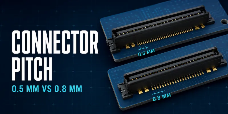
Connector pitch—the center-to-center distance between adjacent contacts—is one of the first decisions in a floating board-to-board design. It affects far more than connector width. Pitch changes the usable PCB land pattern, routing escape, solder-paste process window, inspection access, contact system, and available product families.
There is no universally “best” pitch. Select the smallest pitch that meets the electrical and space requirement without exceeding the capability of the PCB, assembly, inspection, and reliability plan.
Quick comparison
| Pitch family | Typical advantage | Main engineering trade-off | Common design question |
|---|---|---|---|
| Fine pitch (about 0.4–0.5 mm) | High pin density and compact board edge | Smaller pads and tighter process control | Can the assembler reliably print, place, inspect, and rework it? |
| Mid pitch (about 0.6–0.7 mm) | Balance of density and routing room | Availability varies by connector family | Does the selected series support the needed SI and travel? |
| Larger pitch (about 0.8–1.0 mm) | More pad area and simpler inspection | Larger connector envelope | Is the extra space acceptable in exchange for more process margin? |
All dimensions, current ratings, and available pin counts must be confirmed on the exact product drawing. Pitch alone does not define electrical capability.
1. Start with system requirements—not a preferred pitch
Before selecting a connector family, define:
- Required signals, grounds, shielding, and current per contact
- Total pin count, future expansion, and keying requirements
- Maximum connector envelope and required board-to-board height
- Float/travel requirement and number of connectors per board pair
- PCB layer count, impedance-control needs, and escape-routing space
- Assembly process, stencil capability, placement accuracy, AOI/X-ray access, and rework policy
- Environmental loading and target product life
This prevents a common mistake: choosing a dense connector first, then discovering it cannot be routed, tested, or assembled with acceptable yield.
2. Fine-pitch connectors: when density is worth the process control
Fine-pitch floating B2B connectors can help camera modules, compact sensor electronics, portable instruments, and other tightly packaged products. They can reduce board area and enable higher pin count in a limited width.
The trade-off is a narrower manufacturing window. A small change in pad geometry, solder-paste volume, stencil alignment, placement offset, or board coplanarity can affect yield more than it would on a larger-pitch part.
Fine-pitch checklist
| Area | Questions to close before release |
|---|---|
| PCB layout | Is the supplier-recommended land pattern used without modification? |
| Stencil | Does the aperture design provide repeatable paste release at the selected pitch? |
| Placement | Are local fiducials, component recognition, and machine capability validated? |
| Inspection | Can AOI identify bridges and opens at this pitch? Is manual inspection defined? |
| Rework | Can the production partner remove and replace the connector without damaging pads or the float mechanism? |
3. Mid-pitch connectors: a balance of density and routing
Mid-pitch options often make sense when the design needs more room around contacts for routing, isolation, or assembly while retaining a compact connector width. They can be attractive for mixed-signal industrial electronics, automotive modules, and designs with controlled-impedance routing.
High-speed performance does not follow pitch alone. A connector’s geometry, ground strategy, pin assignment, stub length, PCB stack-up, and channel length all affect insertion loss, return loss, and crosstalk. Request S-parameters or application-specific test data for the selected connector and validate the complete channel.
4. Larger-pitch connectors: use the available process margin
Where the product envelope allows it, a larger-pitch connector often offers practical benefits:
- Larger solder lands and visual inspection area
- More routing space between adjacent signals
- Easier stencil design and paste-volume control
- Better access for probing, repair, or selective test points
- Potentially more robust mechanical retention features
These benefits do not automatically make the connector suitable for high current or harsh vibration. The appropriate current derating, hold-down style, board thickness, enclosure support, and validation conditions still must be verified for the configured part.
5. Current and power: do not use pitch as a proxy
Contact current capability is affected by contact size, material, plating, number of adjacent loaded contacts, ambient temperature, copper design, airflow, mating condition, and allowable temperature rise. A connector with a larger pitch may still be intended for low-current signal use.
For combined power and signal designs, choose one of the following architectures:
| Architecture | When it works well |
|---|---|
| Hybrid B2B connector with dedicated power contacts | A qualified series provides the required current, creepage/clearance, and derating data. |
| Signal B2B plus separate power connector | Power path requires different wire size, creepage, locking, or serviceability. |
| Multiple contacts in parallel | Only if the manufacturer explicitly permits it and current sharing has been validated. |
Never calculate a power rating by multiplying a single-contact current value without confirming the manufacturer’s derating guidance.
6. High-speed routing considerations
For fast digital interfaces, first allocate contacts and grounds using the supplier’s recommended pin map. Then control the complete path:
- Use a continuous reference plane under the route.
- Route differential pairs to the impedance required by the interface and PCB stack-up.
- Keep pair members matched through vias and layer changes.
- Minimize stubs, unnecessary via transitions, and abrupt geometry changes.
- Keep aggressor signals and switching power away from sensitive pairs.
- Review the connector plus PCB, cable, and receiver/transmitter as one channel.
Targets such as impedance, skew, spacing, and loss budget depend on the interface, board construction, and bit rate. They should come from the system design rules and channel simulation—not a generic connector article.
7. Pitch selection matrix
| Priority | Selection direction | Verification required |
|---|---|---|
| Maximum pin density | Evaluate fine pitch | Fab/assembly capability and rework trial |
| Fast time to stable production | Favor the pitch with a wider documented process window | Stencil, placement, and AOI pilot results |
| High-speed channel | Evaluate qualified high-speed product families | S-parameters and final channel analysis |
| Harsh mechanical environment | Evaluate travel, retention, board support, and test evidence | System-level vibration/shock testing |
| Mixed power and signal | Evaluate a hybrid or separated power path | Current derating and thermal test |
| Low PCB layer count | Consider routing escape and return-path continuity | Layout review before part release |
FAQ
Is 0.8 mm always more reliable than 0.5 mm?
No. Both can be reliable in their intended application. Reliability depends on the specific contact system, footprint, process control, board support, and environmental validation.
Can a fine-pitch floating connector be used in industrial equipment?
Yes, if it meets the mechanical, environmental, current, and assembly requirements. The design team should validate it against the real manufacturing and service conditions.
Which pitch is best for high-speed data?
Choose a connector family with verified channel data for your interface. Pitch is only one geometric variable; the connector architecture and pin assignment are equally important.
Request a pitch and footprint review
Share the target pin count, maximum connector envelope, board stack-up, signal interfaces, current per contact, mated height, travel requirement, and proposed PCB layout. The GSConn engineering team can then recommend actual part numbers and the matching land-pattern and assembly documents.
Related articles: Complete Floating B2B Guide · Float Range Selection · PCB Layout & Assembly · Stacking Height Selection
Related reading on GSConn
Engineering references
- Product-specific footprint, reflow, derating, and signal-integrity documentation
- PCB fabricator and EMS process-capability data
- System signal-integrity design rules and acceptance criteria